NA34 (~1985-1996)
|
Nick DiGiacomo, Hubert van Hecke, Barbara Jacak, Pat McGaughey, Walter Sondheim, Jules Sunier
|
|
| Links:
a page at Lund
|
|
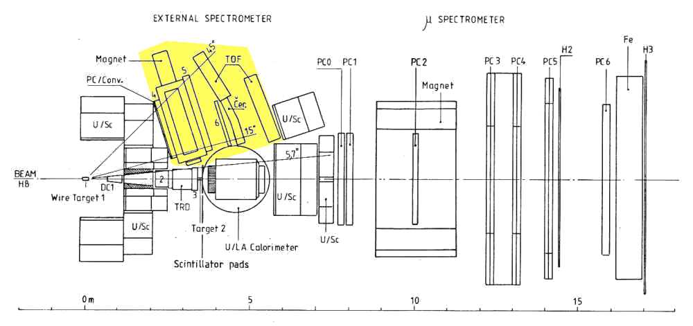
| Experiment NA34 (Helios), was one of 2 big survey experiments
(the other one was NA35) built for the new CERN heavy ion program. CERN
delivered oxygen, sulphur and lead beams, as well as protons.
We built a hadron spectrometer,
highlighted in the picture, which
viewed the target through a narrow slit in the calorimeter wall surrounding the
target area. We built drift chambers, aerogel threshold cherenkov counters and
a scintillator TOF wall.
| 
|
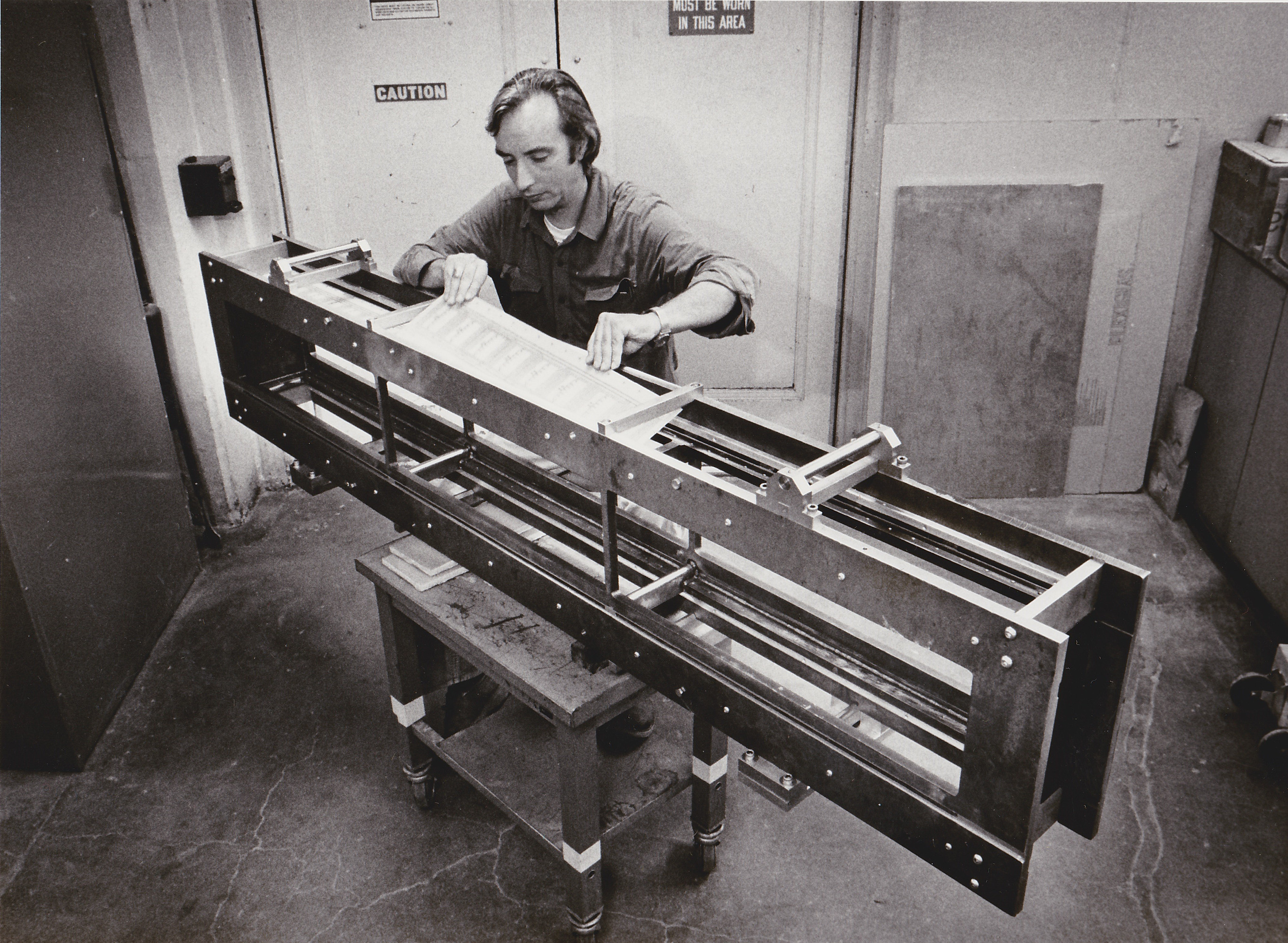
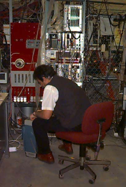
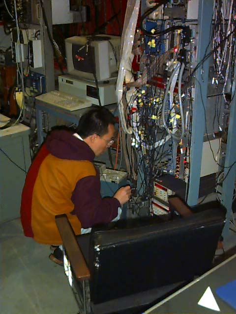
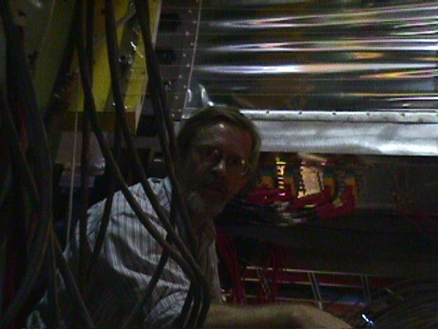
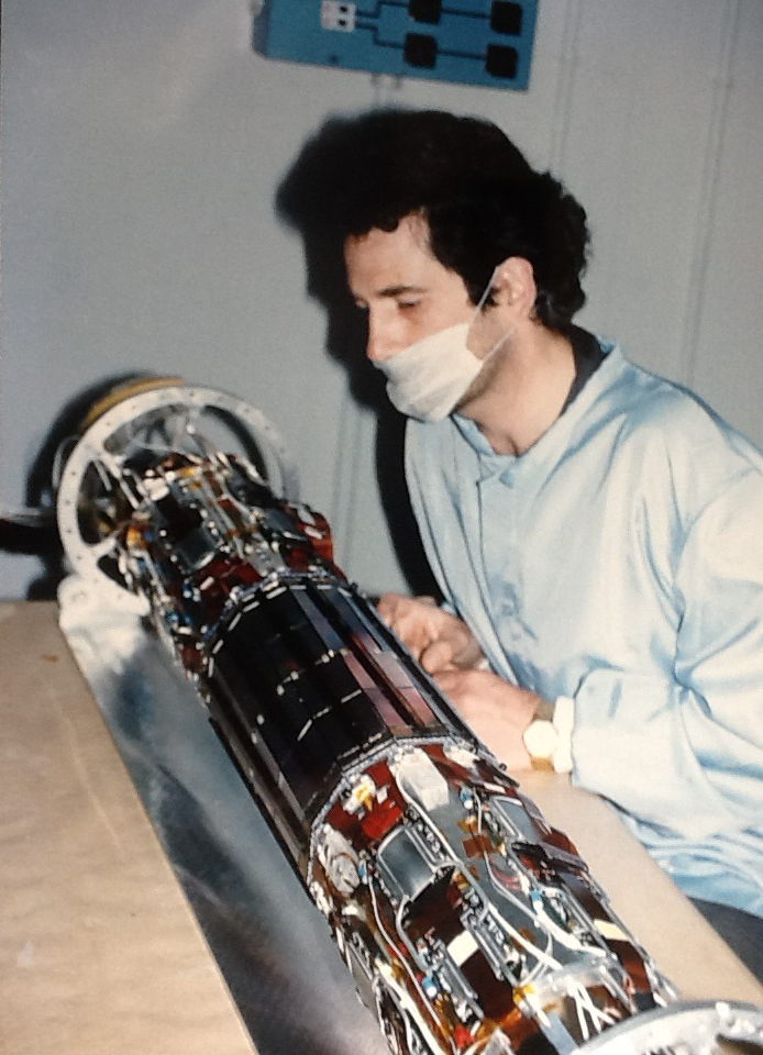
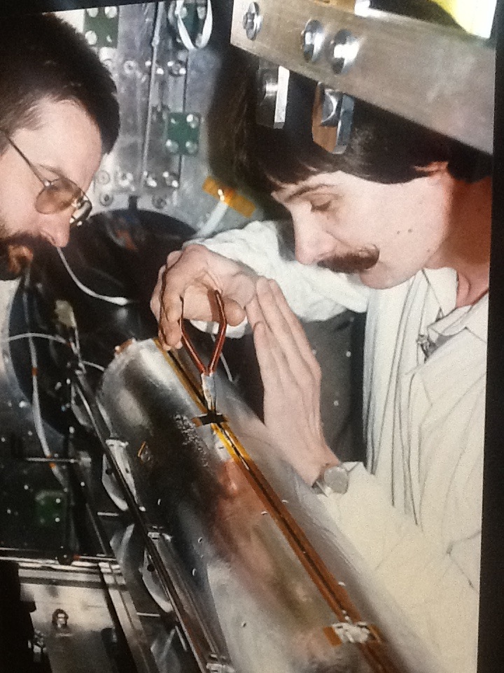
| Walter assembling the drift chamber
| 
|
.
.....lots more pictures, so I put them on
a separate page
|
|
NA44 (~1989-1996)
|
Jan Boissevain, Doug Fields, Allan Hansen, Barbara Jacak, Michael Murray,
Martin Sarabura, Jehanne Simon-Gillo, Walter Sondheim, John Sullivan,
Hubert van Hecke, Nu Xu
|
|
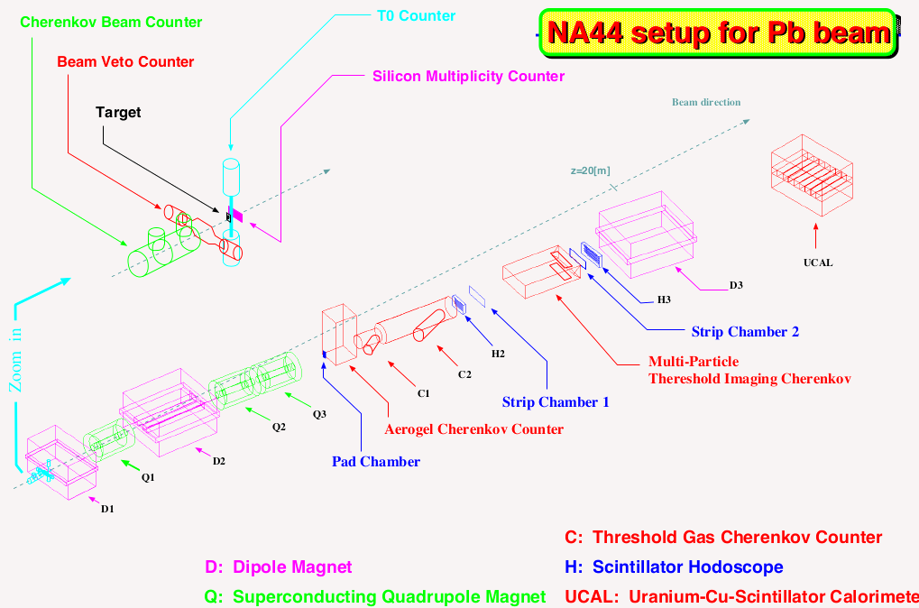
| NA44 (homepage here)
was a second-generation HI experiment. This was a
small-acceptance spectrometer optimized for identified single-particle and
two-particle (Bose-Einstein) distributions.
We built gas cherenkov threshold counters, an aerogel cherenkov counter
and a scintillating fiber T0 counter.
| 
|
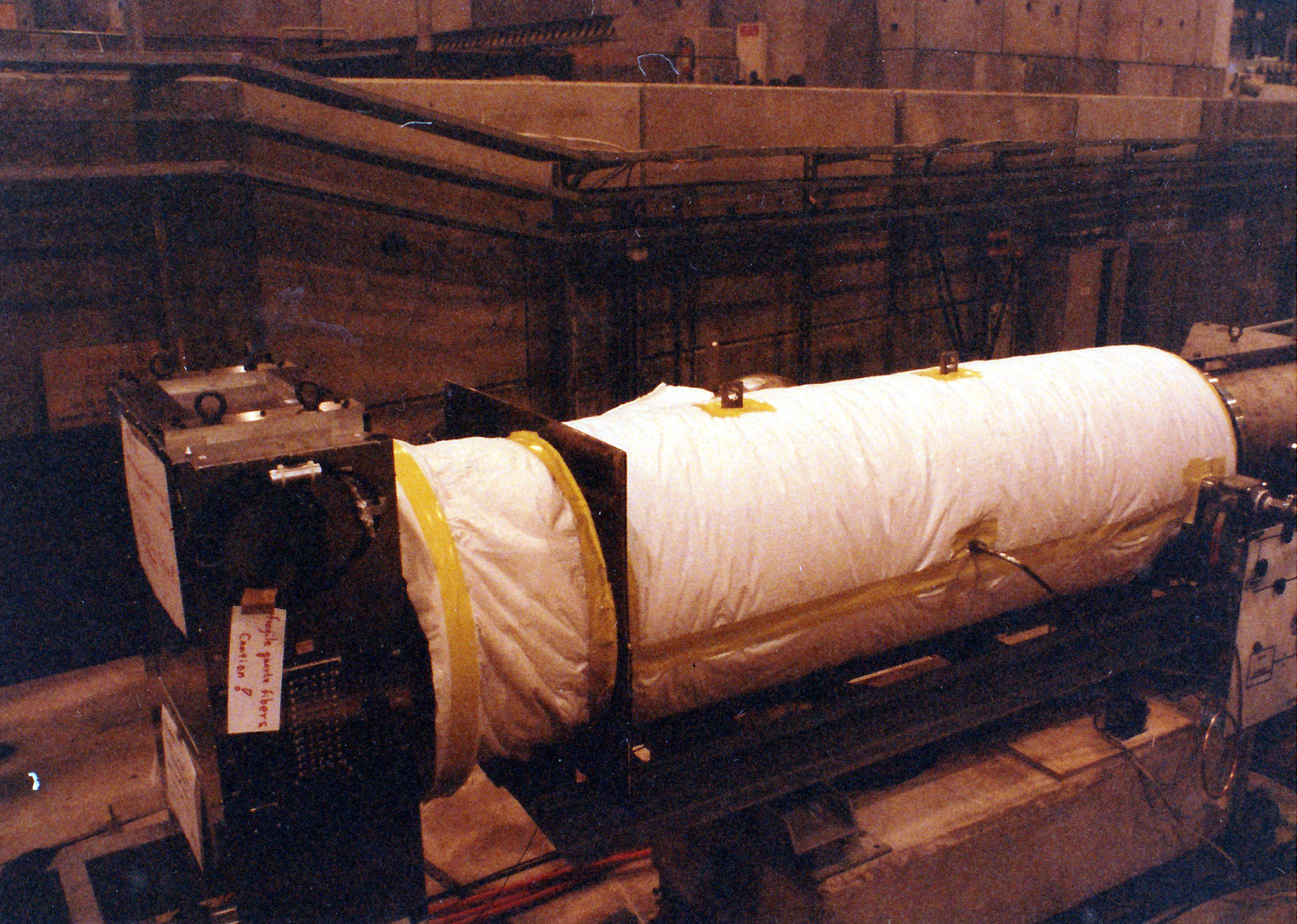
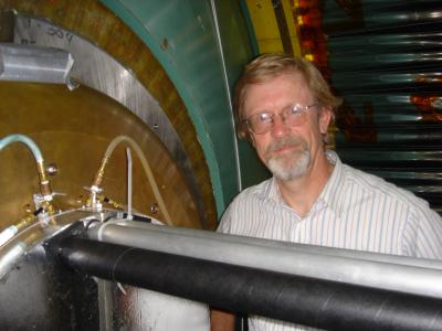
| This is one of the pressurized gas threshold cherenkov counters.
They are kept warm and are wrapped in a blanket.
| 
|
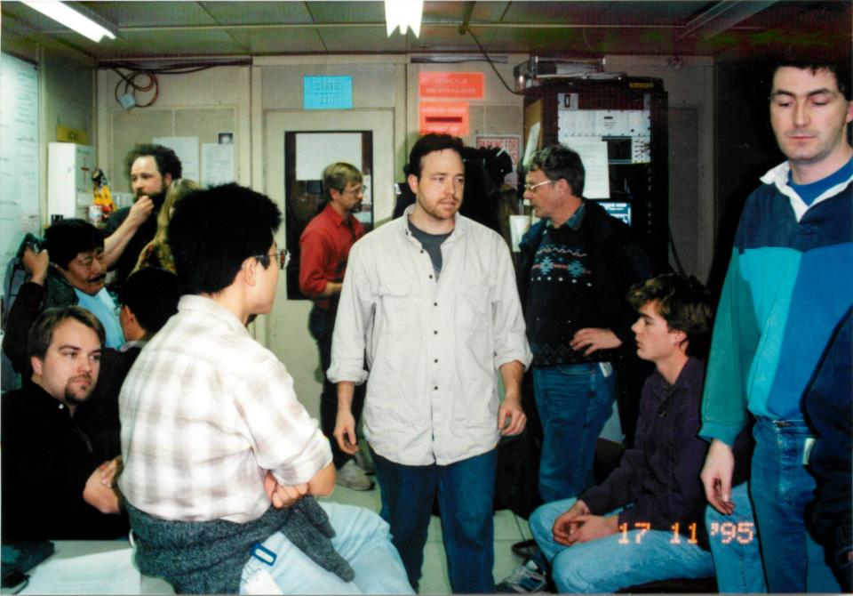
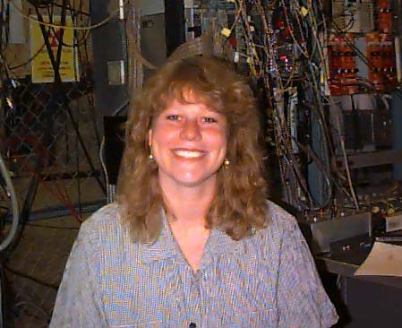
In the NA44 control room:
Ian Bearden, Toru Sugutate, Nu Xu, Achim Franz, Jehanne Simon-Gillo, Masashi Kaneta, Hubert van Hecke,
Dan Zachary, Hans Boggild, Dave Hardtke, Michael Murray.
..... many more pictures,
on a separate page
| 
|
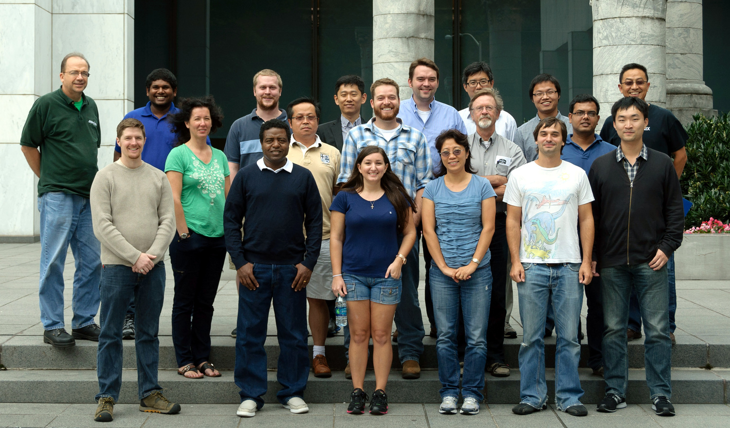
PHENIX/MVD
|
Jan Boissevain,
Tom Carey,
Allan Hansen,
Hubert van Hecke,
Barbara Jacak,
Jo Kapustinsky,
John Lillberg,
Larry Marek,
Pat McGaughey,
Ben Norman,
Jehanne Simon-Gillo,
Walter Sondheim,
John P. Sullivan,
Gary Smith
|
|
|
MVD home page
Chuck Britton (top) and Nance Ericson (middle) from Oak Ridge National Lab arrive at
Los Alamos National Lab with the prototype electronics that will be studied in the
beamtest. Hubert van Hecke (bottom) set up the prototype DAQ system which reads out the electronics.
| 
|
| Hubert van Hecke (shown) and David Jaffe from UCR setup the prototype PHENIX
DAQ for reading out the silicon detector electronics assemblies.
| 
|
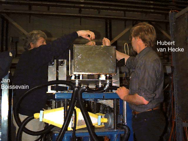
| Jan Boissevain and Hubert van Hecke are installing the prototype MVD RF enclosure
over the silicon detectors and electronics. The shield is constructed of a lightweight
foam, Rohacell, and aluminum foil. One of the objectives of the beam test was to study
the electrical properties of the RF enclosure. A more robust shield (for diagnostic purposes)
fits over the Rohacell enclosure.
| 
|
| Jehanne Simon-Gillo, MVD beam test spokesperson
| 
|
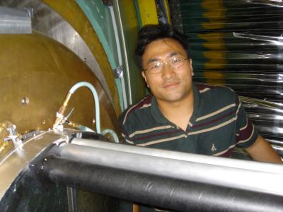
| Jon Kapustinsky studying detector and electronics response
| 
|
| Stringing cables at the AGS test beam
| 
|
| Hubert van Hecke working on the DAQ
| 
|
| Nu Xu looking at response of detector and electronics
| 
|
| Jehanne Simon-Gillo setting up the LVL1 trigger
| 
|
| Hubert and Chi examining the printed circuit MCM
| 
|
| Toshi Shiina mounting an inner top assembly
| 
|
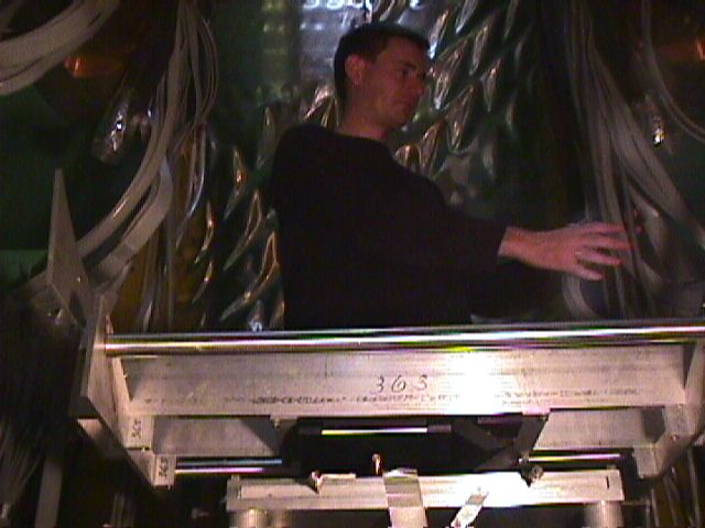
| Hubert after the MVD installation (3:03 AM)
| 
|
| Allan Hansen with the MVD istallation fixture
| 
|
| Finishing the 2005(?) partial MVD installation
| 
|
| Ihnjea Choi finishing the 2005(?) patrial MVD installation
| 
|
PHENIX/FVTX
|
Christine Aidala,
Jan Boissevain,
Melynda Brooks,
Matt Durham,
Jin Huang,
Jon Kapustinsky,
Gerd Kunde,
Kwangbok Lee,
Dave Lee,
Ming Liu,
Pat McGaughey,
Cesar da Silva,
Walter Sondheim,
Hubert van Hecke,
Xiaodong Xiang,
Zhenyun You,
|
|
| FVTX home page
|
|
| .... lots more pictures
separate page
|
|
L3/SMD (~1990-1998)
|
Melynda Brooks, Tom Coan, Jon Kapustinsky, Wayne Kinnison, Dave Lee, Geoff Mills
|
|
|
In 1990, with the support and encouragement of LANL Associate Director,
Gary Sanders, our LANL group joined two research efforts with MIT Professor
and L3 spokesperson, Sam Ting. One of them was to provide broad support to
build a silicon inner tracker for the experiment L-Star, which was proposed
for the Superconducting Super Collider. The second was to join the L3
collaboration at CERN and participate in the design, assembly, installation
and operation of a silicon inner tracker upgrade to the experiment. The
Silicon Microvertex Detector, SMD, was designed as a 2-layer, double-sided
barrel detector [1]. Topside strips were oriented along the beam direction,
and bottom side strips were oriented orthogonal to the beam direction. The
basic detector unit, called a ladder, was comprised of two independent
silicon detectors that were read out on opposite ends of the barrel. They
were joined together as one ladder. In total, there were 24 ladders
comprised of 96 silicon sensors. The sensors were fabricated at
CSEM-Neuchatel, Switzerland. Our main contribution to the project was to
provide the front-end readout for the detector. The schedule to complete
the detector was very aggressive, and so we chose to build based on
technologies that had already been fielded, in particular, from the
Fermilab Tevatron experiment CDF. The SVX readout chip had been designed
for CDF, however, in the first year of running, it proved vulnerable to
radiation damage. A rad-hard version had been designed, but not yet
fabricated. Our LANL group oversaw the first fabrication runs of that
chip, which was called SVX-H. There were also strict constraints to run
the SMD at 20 degrees Celsius. In order to accomplish that, we decided to
change the hybrid substrate from the alumina used by CDF, to a much more
thermally conductive material, aluminum nitride. Sophisticated modeling by
the mechanical engineering group at LANL guided the cooling design and
thermal contact between hybrids and cooling channels [2]. The multilayer
hybrid, thick film printed with alternating conductor and dielectric,
required 34 individual prints and 23 firings. Unexpectedly, the high
thermally conducting substrate caused the dielectric to craze during the
elevated temperature processing, causing the metal layers to be unstable.
It took several iterations of development with the ink producers, Ferro
Corporation, before we were able to find a stable dielectric paste. The
hybrids were fabricated at Promex in Santa Clara, California. The SVX-H
die were wafer probed at LBL. The assembled hybrids were qualified at LANL,
shipped to CERN, and tested again after they arrived. LANL also designed the
kapton readout cables that connected the hybrids to the converter boards.
At CERN, LANL participated in the testing, assembly, installation and
commissioning of the SMD. A core team of four people were allowed into
the restricted area in the 'pit' to install the SMD in March-April 1993,
LANL was represented on that team and had the role of detector specialist,
alongside the operations specialist and 2 CERN technicians.LANL also had the
role of Deputy Project Leader of the SMD and reported directly to Sam Ting on
his executive council. The LANL group collaborated on L3 for the remainder of
the decade.
[1]
Design and Construction of a Double-sided Silicon Vertex
Detector for the L3 Experiment at CERN, J.S. Kapustinsky et. al., IEEE
Transactions on Nuclear Science, Volume 41, Issue 4, pg. 772, 1994.
[2]
Heat Transfer Using Aluminum Nitride in a Silicon Microvertex Detector,
J.S. Kapustinsky and Eric Perrin, Proceedings of the Ist International
Conference on Detector Cooling, Lausanne, Switzerland, Oct 4-7, 1994.
Movie of the SMD construction and installation (9 minute mp4)
Overview of L3
|
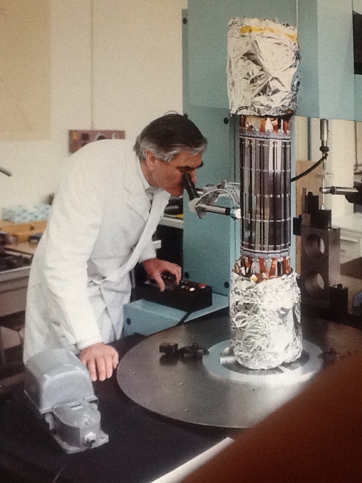
| Jon Kapustinsky
assembling the SMD at CERN in the spring of 1993
| 
|
|
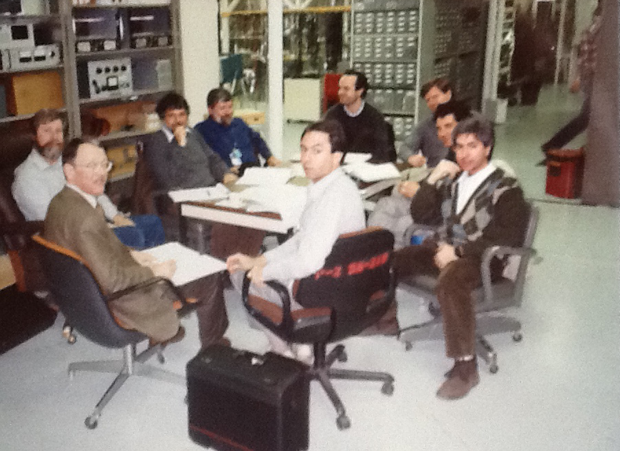
L3 SMD planning meeting that was held at LANL, I think in 1992.
Clockwise from the front is: Michel Lebeau, LAPP-Annecy, Jan Boissevain,
LANL, Eric Perrin, U of Geneva, Wayne Kinnison, LANL, Gian Mario Bilei,
INFN U of Perugia, Geoff Mills, LANL, Jon Kapustinsky, LANL,
Bruno Checcuci,
INFN U of Perugia, Tim Thompson, LANL.
|
|
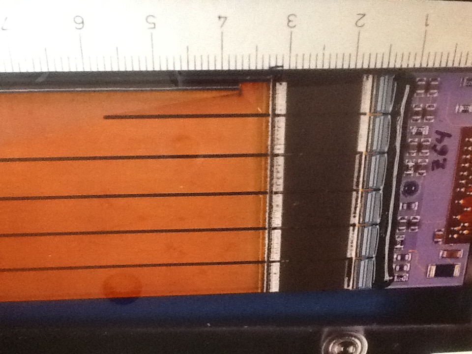
| Los Alamos major responsibility was to provide the front end readout
hybrids (blue aluminum nitride boards). Because our schedule was ahead of
CDF, we were the first institution to fabricate the newly designed SVX-H
chip, a radiation hardened version of the original CDF chip which proved
vulnerable in the first CDF run. This is the Zed side of the 2-sided ladder.
The silicon strips run vertically in this view. The very thin kapton cable
that is glued to the silicon routes the signals horizontally to the end of
the ladder. In between the hybrid and the silicon are decoupling capacitors
on a quartz substate.
| 
|
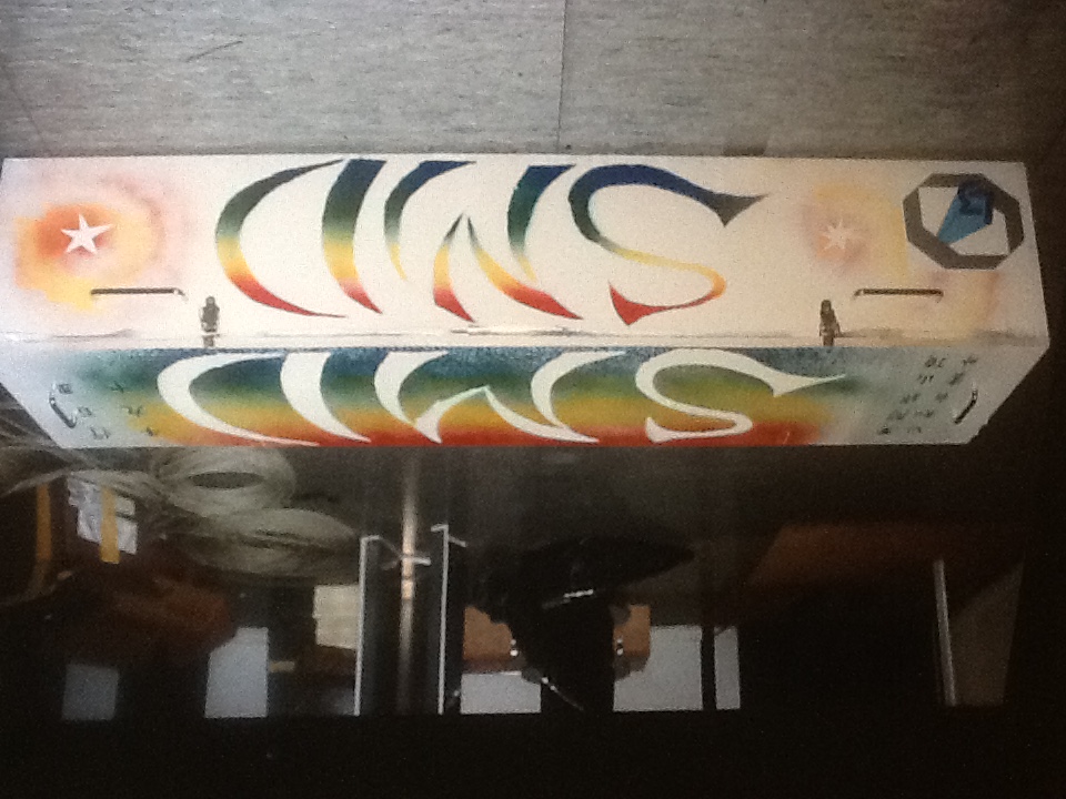
| We (esp. Michel Lebeau) had a custom box built to transport the SMD
from the clean room to the experiment (the pit). The design is in homage to
our spokesperson, Sam Ting.
| 
|
| This is m. Boudineau (CERN) in the metrology lab recording the
dozens of alignment coordinates placed on the detector. Soon after this
picture, he would forget to re-enable a proximity switch, and the optical
head would crash into the detector, damaging 3 ladders. With no time left
to repair, we installed the detector in 1993 and removed, repaired and
re-installed in 1994.
| 
|
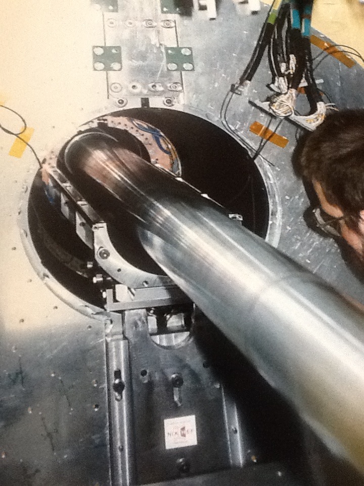
| L3 was the last experiment on LEP to install a silicon detector
and as such, it was an afterthought. The annulus between the beampipe
(beryllium) and the Time Expansion Chamber is the space that was available
for the
detector.
| 
|
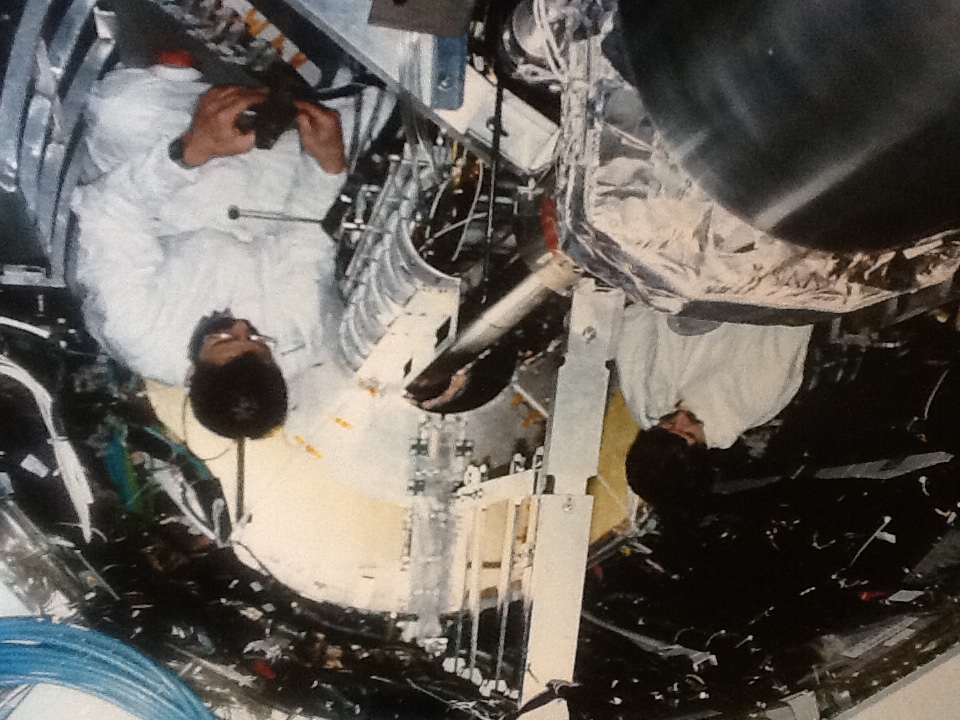
| Two L3 technicians making final preparations to install the
clamshell detector around the beampipe and slide it into place.
| 
|
| Carefully installing the final locking precision pin that holds
the 2 halves of the clamshell together.
| 
|
|