Previous: Flat vs. Cones | Index | Next: Digitization, Occupancy etc.
| In the phnxSili.par file is a variable
sili_endcap_type,
which allows you to choose the endcap configuration. For completeness, I show
all 5 possibilities.
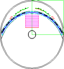
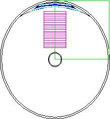
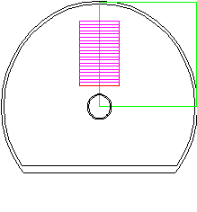
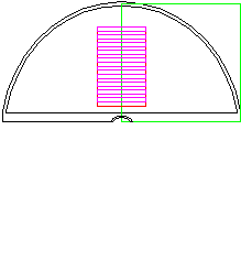
Type 0 is no endcaps at all. Note that for clarity, I haven't drawn the barrel layers, and only the outline of the barrel support structure. The green box shows the +x, +y, +z coordinates. | 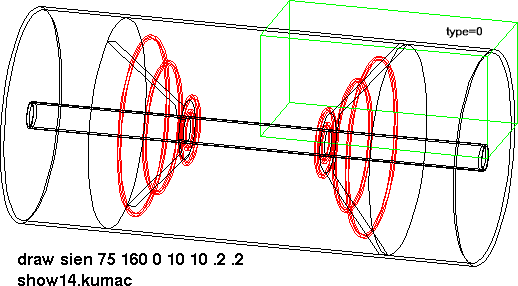
|
| Type 1: tilted panels forming the umbrellas | 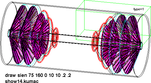
|
| Type 2: flat panels | 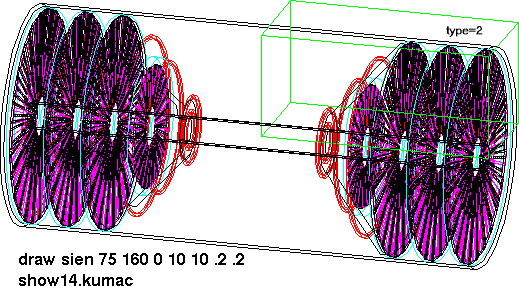
|
| Type 3: tilted LDRD planes | 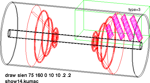
|
| Type 4: flat LDRD planes
The z-position of the planes is such tat they don't interfere with the service cone at low z and the back enclosure at high z for both the straight and rotated configuration. z's are | 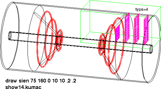
|
| This is a closeup view of the first LDRD plane. There are 2×6 silicon strips, each 73.6×6.4 mm, 300um thick, with 5.6 mm gaps in between. The center-to-center spacing of the front 6 and back 6 strips is 2mm. The bottom edge of the Silicon is 35mm from the nominal beam axis. | 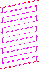
|
| The 12×2 panels exceed the envelope at 17.7 cm. | 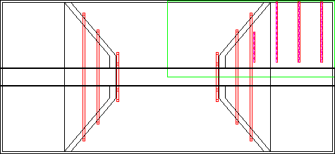
|
| The planes are tilted by 22 degrees, and reduced in height (12,20,20,20 strips respectively). Cross sections
along the blue lines are shown below. In the sections, the green structures are the barrel layers, the blue structures
are the barrel cables, cooling pipes and supports.
The bottom of the planes are at y = 3.5 cm, z = 21.8, 28.0, 33.3, 38.6 cm, tops at y = 10.2, 14.8 cm | 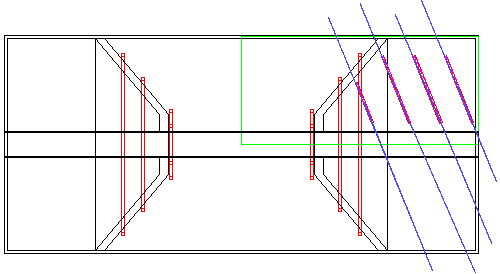
|
| |
phnxSili_04apr06.par
pisa_svx_only.kumac
svx_13apr06.f
| Here are the details. This is a drawing of the first
module, seen edge-on in the z-y plane (not to scale). The dimension in the
x-direction for each of these 8-chip modules is 73.6 mm.
The lowest point of each layer is 3.5 cm from the beamline. Each module, here represented as a single continuous silicon slab, consists of 8 pixel detectors, with 100 (hor) by 28 (vert) pixels each. The pixels are 400×50 um. | 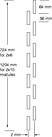
|
back
Previous: Flat vs. Cones | Index | Next: Digitization, Occupancy etc.