|
|
|
| Previous page
| Up to the index
| Next page
| |
|
|
|
| Previous page
| Up to the index
| Next page
| |
1. Brief description of multiplexed serial readout & MAX186 ADC
This is the watchdog of the MVD. All LDO voltage regulator outputs for the front end electronics and the mother board itself, as well as temperature monitoring voltages from each section of electronics, i.e MCMs, power/comm boards and mother boards, which total 93 channels, are readout through 12 MAX186 ADCs per mother board. LDO voltage regulator output monitoring voltages pass through a voltage divider before they arrive at the ADC's, so that divided voltages are readout by the ADC's.
The data acquisition process of the MAX186 ADC using serial communication starts by pulling down the CS-bar line. ( Refer to the product note by the manufacturer[5] ) After CS-bar falls, a control byte is clocked into the DIN line. For the mother board, two binary to decimal encoders pull down one CS-bar line among 12 CS-bar lines accoding to binary chip address, ADC_A0-3. Table 6 shows the control byte format which we used.
| Bit | Name | Value | Description |
|---|---|---|---|
| 7 | START | 1 | Define the beginning of the control byte |
| 6, 5, 4 | SEL2, 1, 0 | See table 7. | These three bits select which of the eight channels are used for the conversion. |
| 3 | UNI/BIP | 1 | Select unipolar conversion mode. An analog input signal from 0V to Vref(4.096V) can be converted. |
| 2 | SGL/DIF | 1 | Select single-ended conversion. In single ended mode, input signal voltages are refered to AGND. |
| 1, 0 | PD1, PD0 | 1, 1 | Select the external clock mode |
![]()
In selecting a channel, the MAX186 ADC has an unusual counting method. This
should be taken into account of when making software interface for the serial
communication.
![]()
| SEL2 | SEL1 | SEL0 | Selected channel |
|---|---|---|---|
| 0 | 0 | 0 | CH0 |
| 1 | 0 | 0 | CH1 |
| 0 | 0 | 1 | CH2 |
| 1 | 0 | 1 | CH3 |
| 0 | 1 | 0 | CH4 |
| 1 | 1 | 0 | CH5 |
| 0 | 1 | 1 | CH6 |
| 1 | 1 | 1 | CH7 |
![]()
After 8 control bits are clocked into DIN, the SSTRB line goes high during
one clock period. Converted data are clocked out from DOUT on each of
the next 12 SCLK falling edges. The external clock should range from
0.1 MHz to 2.0 MHz in order to guarantee the normal operation of the ADC.
In the real MVD, the ancillary system will control the
multiplexed serial readout process to acquire data from the MAX186 ADCs on
the mother boards.
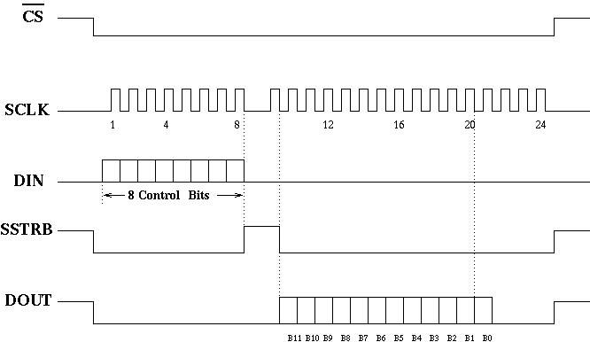
Fig 7. MAX186 ADC Conversion Timing
2. Setup & procedure
The setup consisted of two main parts. A LeCroy 2366 -> ECL-NIM converter -> Level Adapter chain is used to address the output channel and send serial control signals. The other part reads and displays the data-out using a NIM-IN module. Data readout starts by setting or resetting each binary chip address line,ADC_A0-3. Then 8 control bits clock into DIN through the LeCroy 2366 -> ECL-NIM converter -> Level Adapter chain. After one click, the ADC sputters out the converted data, while MSB comes out first. These 12 bits flow into NIM IN to be readout and displayed by a user interface residing on a HP-UX.
| Level Adapter | monitoring signal connector |
|---|---|
| ch 1 | pin 8, ADC_A0 |
| ch 2 | pin 10, ADC_A1 |
| ch 3 | pin 12, ADC_A2 |
| ch 4 | pin 14, ADC_A3 |
| ch 5 | pin 5, serial data in |
| ch 6 | pin 3, serial clock |
![]()
Currently there are two versions of the user interface, in Fortran and C. The Fortran source file is /usr1/mvdonl/camac/ancf.f, and runs very slowly. The serial clock generated by this version is about 1 KHz. The C version,whose source file is /usr1/mvdonl/camac/mbvolt_read.c, can almost make a 50 KHz serial clock. This is much faster than the Fortran version but we still hope to speed up more because the optimum serial clock frequency range is 0.1 MHz - 2.0 MHz. Anyway a user interface repeats the data readout process for all 93 channels, and finally displays the ADC values on screen.
![]()
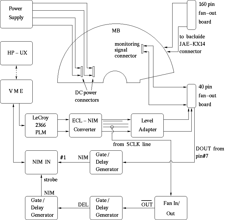
Fig 8. The setup for the multiplexed serial readout test
As a preliminary test, we powered up the mother board and readout ADCs, which is supposed to turn out 3 non-zero ADC values from the 5th chip and 6 non-zero values from the 11th chip corresponding to 3 mother board power monitoring voltages and 6 mother board temperature sensor outputs. To test all channels, the DC power of each group was powered up one by one and at the same time some DC voltage was applied at TEMP_MON pins on the 160 pin fan-out board while ADC values were readout in each case. TEMP_MON pins were assigned as follows.
3. Simple analysis of test results & simulating fault situation
Table 9 shows ADC dataout when only DC power for the mother board was supplied. Three non-zero ADC values on chip# 5 are for the mother board power monitoring voltages, MB_5VD_MON, MB_5VA_MON, MB_-5VA_MON. As we noticed in the LDO voltage regulator test, these monitoring voltages are half of the original voltages(for -5VA_MON, divided by four while the lower potential level is at -5V and the higher level is at +5V). The MAX186 ADC has a 12 bit resolution and the reference voltage Vref is 4.096V. Therefore one ADC channel corresponds to 0.001V. Conclusively, each ADC value means 2.336V, 2.346V, 2.321V of monitoring voltage. We can calculate original output voltages with the monitoring voltages if we take into account the voltage dividers at the output stages of the LDO voltage regulators. For example, 4.672V, 4.692V, -4.792V are the calculated original outputs from LDO regulators for the above three monitoring voltages.
| chip # | CH0 | CH1 | CH2 | CH3 | CH4 | Ch5 | CH6 | CH7 |
|---|---|---|---|---|---|---|---|---|
| 1 | 0 | 0 | 0 | 0 | 1 | 0 | 0 | 0 |
| 2 | 0 | 0 | 0 | 0 | 0 | 1 | 0 | 0 |
| 3 | 0 | 0 | 0 | 0 | 0 | 1 | 0 | 0 |
| 4 | 0 | 0 | 0 | 0 | 0 | 0 | 0 | 0 |
| 5 | 0 | 0 | 0 | 2336 | 2346 | 2321 | 0 | 0 |
| 6 | 0 | 0 | 0 | 0 | 0 | 0 | 0 | 0 |
| 7 | 0 | 0 | 0 | 0 | 0 | 0 | 0 | 0 |
| 8 | 0 | 0 | 0 | 0 | 0 | 0 | 0 | 0 |
| 9 | 0 | 0 | 0 | 0 | 0 | 0 | 0 | 0 |
| 10 | 0 | 0 | 0 | 0 | 0 | 0 | 0 | 0 |
| 11 | 592 | 592 | 592 | 596 | 597 | 592 | 0 | 0 |
| 12 | 0 | 0 | 0 | 0 | 0 | 0 | 0 | 0 |
Six non-zero ADC values on chip# 11 correspond to outputs from six temperature sensors on the motherboard. There is a formula for the temperature sensor to convert the output voltage to the temperature.
V is the output voltage from the temperature sensor and T is the temperature. Hence the estimated temperature of the mother board was around 23 degrees which is close to room temperature. Also we could see the increase of ADC values corresponding to temperature sensor outputs by heating the temperature sensors.
As a second step of the test, we powered up group 1 with one more power connector and applied +0.548V at the G1_MCM1_TEMP_MON pin as well as, the PC1_TEMP_MON pin on the 160 pin fan-out board. In this case, the ADC readout results are shown in table 10.
| chip # | CH0 | CH1 | CH2 | CH3 | CH4 | Ch5 | CH6 | CH7 |
|---|---|---|---|---|---|---|---|---|
| 1 | 2314 | 2304 | 2336 | 2336 | 1170 | 0 | 0 | 0 |
| 2 | 0 | 0 | 0 | 0 | 0 | 0 | 0 | 0 |
| 3 | 0 | 0 | 0 | 0 | 0 | 0 | 0 | 0 |
| 4 | 0 | 0 | 0 | 0 | 0 | 0 | 0 | 0 |
| 5 | 0 | 0 | 0 | 2337 | 2346 | 2321 | 548 | 2 |
| 6 | 0 | 0 | 0 | 0 | 0 | 0 | 0 | 0 |
| 7 | 0 | 0 | 0 | 0 | 0 | 0 | 0 | 0 |
| 8 | 0 | 0 | 0 | 0 | 0 | 0 | 0 | 0 |
| 9 | 0 | 0 | 0 | 0 | 0 | 0 | 0 | 0 |
| 10 | 0 | 0 | 0 | 0 | 0 | 0 | 0 | 0 |
| 11 | 596 | 585 | 597 | 594 | 594 | 593 | 545 | 0 |
| 12 | 0 | 0 | 0 | 0 | 0 | 0 | 0 | 0 |
![]()
![]()
We did similar tests for all 7 groups and confirmed that all ADC channels turned
out monitoring values. After these tests some interesting tests to simulate
fault situations were implemented
to watch changes in the ADC output values.
The observed changes are summarized in Table 11.
| Fault situation | Description about changes |
|---|---|
| mother board +5VD ---> +4VD | only a ADC value, MB_5VD_MON decreased to 2081 |
| mother board +5VD ---> +3.5VD | Six ADC values, MB_TEMP_MON1-6 went down to 0. So if LDO regulator output for MB_+5VD drops to 3.5V, temperature sensors won't work. |
| mother board +5VD ---> +3.0VD | In this case whole channels showed 0 output values. This means MAX186 ADC doesn't work with 3.0V supply. |
| mother board +5VA ---> +4VA | Two monitoring ADC values, MB_5VA_MON and MB_-5VA_MON decreased at the same time because of the voltage divider. |
| mother board -5VA ---> -4VA | A monitoring ADC value, MB_-5VA_MON increased to 2708. The directly measured monitoring voltage was 2.718V. |
| mother board -5VA ---> -3.5VA | A monitoring ADC value, MB_-5VA_MON changed to 2577 but the directly measured monitoring voltage was 2.843V. |
| mother board -5VA ---> -3.0VA | A monitoring ADC value, MB_-5VA_MON changed to 2576 but real input to this channel was 2.966V. |
| mother board -5VA ---> -2.0VA | Though real input to MB_-5VA_MON channel increased to 3.229V, the ADC output value from this channel decreased to 2194. |
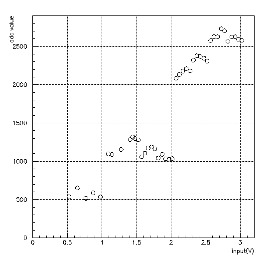
Strangely enough, in the last three cases we got invalid ADC output values. Above approximately 2.8V, the ADC value started dropping. From this result we decided to check the ADC response for inputs of a wide range. We applied voltages with an interval of around 0.05V on TEMP_MON pins on the 160 pin fan-out board and readout ADC. The ADC response(Fig.9) showed more dropping points. It looks like that ADC worked normally only for very narrow ranges around 0.5V, 2.1V, and 2.3V inputs. We guess that this abnormal ADC response is due to the relatively slow serial clock which was generated by both versions of the user interface. Further tests on ADC response should be done with the serial clock frequency faster than 0.1MHz and slower than 2.0MHz.