|
|
|
| Previous page
| Up to the index
| Next page
| |
|
|
|
| Previous page
| Up to the index
| Next page
| |
1. Brief description about analog spy
A mother board provides 42 analog spy line pairs, where one pair consists of the preamp spy and the AMU spy from one MCM. This is done using the ANALOG DEVICES 16 channel analog multiplexer ADG406[4]. A total of six ADG406s per mother board take 42 analog spy signal pairs from 42 MCMs in seven groups. In fact, there are 96 channels but two channels from each chip go to the AGND. These 'dead' channels are placed between six spy-out channels of one group. By sending six address bits, so called SPY_A0-5, through the monitoring signal connector , we can switch the spy output channel. Two enable bits, SPY_A4-5, enable one pair of ADG406 and four address bits, SPY_A0-3, select one channel from sixteen channels to be sent out to the MVD Ancillary System.
ADG406 has two operation modes, single or dual supply mode. For the mother board, ADG406 will be operated in dual supply mode with a +5V and -5V supply, which means that input analog signal ranges from -5V to +5V. The output of the ADG406 is an inverted analog signal with gain 1.
2. Setup & procedure
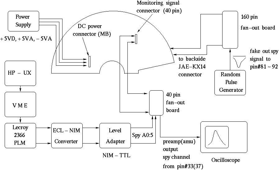
Fig 5. The setup for analog spy channel test
To switch analog spy channels each address line should be set or reset independently. A CAMAC logic module(LeCroy 2366) was used to output logic 1 or 0. Because the ADG406 recognizes TTL level logic, through two logic level converters, six address bits were sent. Six channels from NIM to TTL converter were connected to the 40pin fan out board by lemo cables of which one ends was cut off and soldered onto pins 19-24 of the fan out board.
| Level Adapter | Monitoring signal connector |
|---|---|
| ch 1 | pin 19, SPY_A0 |
| ch 2 | pin 20, SPY_A1 |
| ch 3 | pin 21, SPY_A2 |
| ch 4 | pin 22, SPY_A3 |
| ch 5 | pin 23, SPY_A4 |
| ch 6 | pin 24, SPY_A5 |
A fake out_spy signal(width - about 5 micro sec) was generated with a random pulse generator. We tested both polarities up to 5V in amplitude. There is a user interface to control the logic module so called analog_spy.o, running on the VME cpu. The source is /usr1/mvdonl/camac/ analog_spy.c on mvdonl. The whole procedure of the test is as follows.
3. Analog spy test result
The functions of all spy channels were verified. The analog spy output was inverting the signal with an approximate gain of 0.88. Though the calculated gain was smaller than the ideal gain of 1.0, there was no significant distortion of the output waveform and no saturation of the output signal for input amplitudes up to 5V. Similar responses were observed from all six ADG406 chips. That is, there was no measurable fluctuation of output through whole channels for the same input signal. The fitting in Fig 6 is from the data of group 1, MCM 1 channel. Minus slope means inverted outputs and the fitting parameter P2 is the calculated gain. It shows a definite linear response.
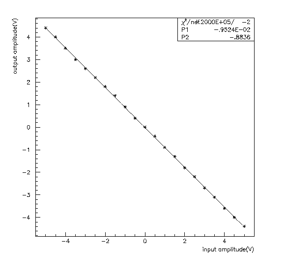
Fig 6. Linear response of an analog spy channel( postscript version )