![[multiplexed serial readout...]](../../../gifs/arrow.marble.left.gif)
|
![[introduntion]](../../../gifs/arrow.marble.up.gif)
|
![[conclusion]](../../../gifs/arrow.marble.right.gif)
Previous page
| Up to the index
| Next page
| |
![[multiplexed serial readout...]](../../../gifs/arrow.marble.left.gif)
|
![[introduntion]](../../../gifs/arrow.marble.up.gif)
|
![[conclusion]](../../../gifs/arrow.marble.right.gif)
Previous page
| Up to the index
| Next page
| |
1. Brief description about the PECL clock
PECL logic has relatively narrow swinging voltage for better high frequency performance. Typical ECL logic definition is as follows.
In the meantime, generally PECL logic "0" and "1" have 5V offset above ECL logic level with the swinging voltage of 0.9V.
A PECL clock with 4X beam clock frequency(about 38MHZ) is used for AMUADCs on the MCMs to keep the integrity of sensitive input signals which come from preamps. On the mother board there is a TTL to PECL translator, so called SY10ELT22, to make a pair of differential PECL clocks and next to it a fan-out buffer, so called SY10E111, to distribute a pair of differential PECL clocks over six power/comm boards and one daughter board. Also on the power/comm board( or daughter board ) there is a fan-out buffer to send out a pair of differential PECL clocks coming from the mother board over six MCMs to reach the final destination.
![]()
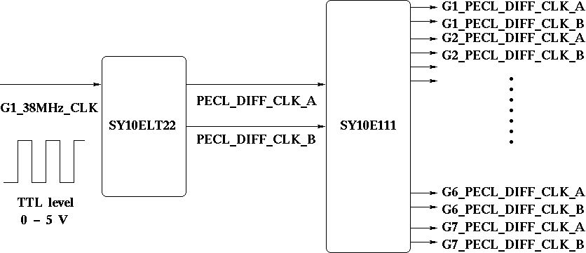
Fig 10. TTL to PECL translator & Fan-out buffer on the mother board
2. Setup
![]()

Fig 11. The setup for the PECL clock test
The setup is rather simple. TTL clocks with various frequencies from a pulse generator enter into pin 17 of the group 1 timing & control signal. A lemo cable from a pulse generator delivers the TTL clock, whose one end is cut off and soldered onto pin 17 of the 20 pin fan-out board. For better impedance matching, a terminator resistor is soldered between the TTL clock line and the ground because it seemed to us that the fan-out board and the ribbon cable connected to it caused the signal to be reflected at the joint.
After powering up the mother board, output differential PECL clocks for each group were monitored from pins 13 and 15 on the 160 pin connectors(J36-J41). In case of the PECL clocks of group 7, it's monitored from pins 13 and 15 on the 80 pin connector(J35). Actually, output PECL clocks were taken through the 160(or 80) pin fan-out board and lemo cables which were soldered onto fan-out boards.
3. Results of the PECL clock test
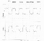
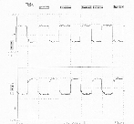
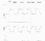
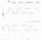
Tentatively we observed PECL outputs at relatively low frequencies(5MHz, 10MHZ, 20MHz, 30MHz) and moved onto the 4X beam clock frequency. Output PECL clock waveforms at low frequency, 10 and 20MHz, are shown in Fig 12. Upper and lower waveforms represent one pair of PECL differential clock(A,B). PECL clocks for groups 1-6 resembled each other and PECL clocks for group7 had a different shape. These PECL clocks swung from 3.0 to 3.9Volt.
|
|
|
|
| a)10MHz,group6 | b)10MHz,group7 | c)20MHz,group6 | d)20MHz,group7 |
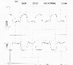
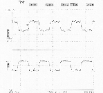
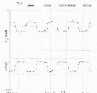
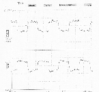
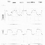
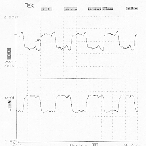
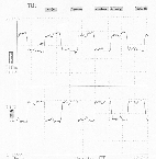
PECL differential clock outputs for all 7 groups at 4X beam clock frequency, i.e 38MHz, appear in Fig 13. Again the upper waveform represents PECL differential clock A and the lower one represents the counterpart of it, PECL differential clock B. At large, these PECL clocks had 0.8V of the swinging voltage, with top levels at 3.9V and bottom levels at 3.1V. 0.8V of the swinging voltage is the acceptable minimum as PECL. Needless to say, PECL clock frequencies were 38MHz for the 38MHz TTL input. At this frequency some output clocks showed an asymmetry between the top and bottom portion of the waveform as well as ripple but these were not significant.
|
|
|
|
| a)38MHz,group1 | b)38MHz,group2 | c)38MHz,group3 | d)38MHz,group4 |
|
|
|
|
| f)38MHz,group5 | g)38MHz,group6 | h)38MHz,group7 |