Each of the two DAC serial ports talks to 3 8-bit DACs, each one of which has 4 output channels (A-D), for a total of 24 settable voltages. Only DAC2 was present during the test. Full scale on these DACs was 5V. An added complication is that the data line is chained through the three chips, whereas the clock, load and cs-bar lines are parallel, as in figure 4.
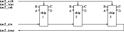
Figure 4: Lines to the DAC chips
To program a single FEE DAC chip, a 36-bit package needs to be sent, consisting of 3 12-bit sub-packages, one for each of the three DACs. The first 4 bits of these 12 (labeled A1, A0, C1 and C0), determine which of the 4 channels is to be affected, and the remaning 8 bits correspond to the voltage to be set:
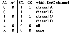
Where 'x' means that the bit can be either 0 or 1. One cannot shift a packet into one chip and strobe the load line without also shifting data through the other chips, and strobing all three chips at the same time. In this context, the 'no-op' command caused lots of confusing behavior of chips. The solution chosen was to save the status for all the bits in the control program, and shift out the entire configuration each time any of the 12 voltages is changed. Thus all voltages are reloaded every time. As an example, the following string of 144 bits sets all voltages to 0, except for channel 3D, which is set to 100\% of full voltage, or 5V.
         ------ A ----  ------ B ----  ------ C ----  ------ D ----
chip 1:  0011 00000000  0111 00000000  1011 00000000  1111 00000000
chip 2:  0011 00000000  0111 00000000  1011 00000000  1111 00000000
chip 3:  0011 00000000  0111 00000000  1011 00000000  1111 11111111
Figure 5 shows the timing of the DAC serial signals.
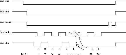
Figure 5: Timing of the DAC serial signals