There are several important constraints on the design of the electronics for
the vertex detector. The size and mass must be minimized to prevent space
conflicts with other detectors and to minimize multiple scattering and
production of secondary particles. The electronics system must produce as
little heat as possible; if the power consumption can be kept to the order of
 1mW/channel, then forced-air cooling should be possible. If air
cooling is not possible, a complicated and potentially expensive cooling system
will be required, which would add significant mass in the vertex region. The
shaping time of the preamplifier must allow individual beam crossings (every
200ns) to be distinguished. Since the vertex detector multiplicity is
expected to form part of the first level trigger, a system which moves this
information "into the pipeline" at this rate is needed. This time constraint,
combined with the power consumption constraint eliminates most of the presently
available electronics components.
1mW/channel, then forced-air cooling should be possible. If air
cooling is not possible, a complicated and potentially expensive cooling system
will be required, which would add significant mass in the vertex region. The
shaping time of the preamplifier must allow individual beam crossings (every
200ns) to be distinguished. Since the vertex detector multiplicity is
expected to form part of the first level trigger, a system which moves this
information "into the pipeline" at this rate is needed. This time constraint,
combined with the power consumption constraint eliminates most of the presently
available electronics components.
| source | Description | Available now? | Where used or to be used | Approx. peaking time (ns) | Power use (mW/chan) | |
|---|---|---|---|---|---|---|
| FNAL6,10 | bipolar | Yes | E789 | 10 |  50 50 | |
| LBL11,24 | SVX-D: shaper, disc., latch., digital circuits, Some rad. damage problems | Yes | CDF (SVX-I) | 700 | 1-2 | |
| FNAL/ORNL25 | R&D: CMOS preamp, shaper, prototype (now), more later | Yes* | BVX (D0), RHIC? | 200 | ||
| LBL26 | SVX-H: rad. hard CMOS, shaper, disc., latch, digital circuits | Yes* | CDF (SVX-II), L3 | 500 | 1-2? | |
| LBL27 | CMOS preamp, shaper, disc, latch, analog sum?, no buffering | No | SDC | 15? | ||
| Santa Cruz28 | No | SDC | ||||
| Ikeda19 | R&D: combined Si strip detector & front-end | Yes* | SDC | 7 | ||
| SDI20 | R&D: BiCMOS combined Si strip detectors & front-end | No |
Table 7: Selected sources of front-end electronics for Si strips vertex detectors. The last two columns gives the approximate peaking time and power dissipation. * indicates that only prototypes are available.
There are several Si strip vertex detectors currently being designed (for
instance for GEM and SDC at the SSC), and some already in operation6,10-15.
As a result, some components are available. However, none of these components
can be considered completely "off-the-shelf" items. Even in those cases where
a similar component has been made before, some modifications will be necessary.
For example, the Si strip detector wafers similar to the ones needed for this
detector have been constructed by a number of vendors16-20. However, in
order to purchase them for use with this detector, a new set of masks must be
made for the appropriate strip pitch and length. Then the detectors must be
manufactured and tested. Quality control is time-consuming, but vital, as is
working closely with the vendors. A well-defined and complete set of
quality-control parameters must be agreed upon with the venor.
For a project of this scale,
automated testing on a probe station will probably be necessary. A custom probe
card and some of the related software would have to be provided. Our
experience suggests that this process typically takes 18 months (or
more) before all of the detector elements are in hand.
The first part of the electronics system is the connection of the detector
strip to the preamplifier. Although some work is being done to integrate the
front-end electronics and the detector strips19-20 on a single wafer, we
expect to have a separate front-end integrated-circuit chip which will be
wire-bonded to the detector strips. Here, the 100 pitch is advantageous
since machines exist for wire-bonding at this pitch. The front-end electronics
chip would consist of a preamplifier, shaper, discriminator, and latch. An
LED-based optical fiber readout system, for high speed (100MHz) and
low local power consumption will probably be used. In order to simplify the
mechanical design, the electronics packages would be supported on the Si
detector chips.
pitch is advantageous
since machines exist for wire-bonding at this pitch. The front-end electronics
chip would consist of a preamplifier, shaper, discriminator, and latch. An
LED-based optical fiber readout system, for high speed (100MHz) and
low local power consumption will probably be used. In order to simplify the
mechanical design, the electronics packages would be supported on the Si
detector chips.
The simulations have shown that it is possible to satisfy all of the vertex
detector's design criteria without using ADC's on the individual strips. This
would simplify the system and reduce the volume of data produced. However, a
single analog output for each detector chip would be useful for triggering. Due
to the angle of incidence problems, a simple sum of the analog signals from
each chip would not give the multiplicity without first determining the
vertex position. For a multiplicity to be used in the trigger, a
sum of discriminator outputs from the strips parallel to the beam (where
1 strip per particle would be "hit") is needed. A sum of
the analog signals from all strips on a chip might be useful; if  is
constant over the length of the vertex detector (based on Fritiof calculation,
this is true at the 15% level --- see fig. 3), then the total energy
loss in each detector would be proportional to independent of the z
position relative to the vertex. This is similar to an observation in the
Oasis Letter of Intent21, although that vertex detector geometry was much
different. This quantity could also be useful in triggering. Knowing
implies knowledge of the multiplicity only if the vertex position is known ---
so if the multiplicity is needed for the first level trigger, the need for
parallel strips remains.
is
constant over the length of the vertex detector (based on Fritiof calculation,
this is true at the 15% level --- see fig. 3), then the total energy
loss in each detector would be proportional to independent of the z
position relative to the vertex. This is similar to an observation in the
Oasis Letter of Intent21, although that vertex detector geometry was much
different. This quantity could also be useful in triggering. Knowing
implies knowledge of the multiplicity only if the vertex position is known ---
so if the multiplicity is needed for the first level trigger, the need for
parallel strips remains.
More work is needed to design, manufacture, and test suitable front-end electronics components. Some work on this subject has been reported at this conference22,23. This important work should lead to front-end electronics systems which are fast enough and have low enough power consumption. A summary of selected electronics systems for Si strip detector appears in table 6. None of the currently available components satisfies the combined power dissipation and speed limitations for this detector. In addition, it is crucial to integrate the components into a system as soon as possible. It would be unwise to start construction of an expensive and complex detector system without careful tests of all of the components together. Some of this integration work is already being done by the P2 group in Los Alamos. Prototype CMOS preamplifiers25 have been acquired and will be combined with an OPAL-type strip detector17, using a locally developed hybrid circuit. Tests of this system will take place in early 1992, with tests of other systems26 following shortly.
The electronics development can take place using either CMOS or bipolar
processes. CMOS circuits are easier and cheaper to develop, but are not
suitable for long strips, which have large capacitance --- this is not a
limitation in the current design, but could be for other designs. It will be
easier to develop circuits with less than 100 pitch using a bipolar
process than with CMOS --- but the current design assumes 100---
eliminating this advantage. In general, bipolar circuits use less power for the
same performance as CMOS.
The radiation damage to a cylindrical vertex detector caused by charged particles
from the primary reaction can be estimated1 by assuming that is
constant over the length of the vertex detector. Assume that a "RHIC year" is
107sec long at a Luminosity29 of 2 x 1026cm-2sec-1 with
 tot = 6.13b. For central Au+Au collisions assume that
for charged particles is
constant at 800 in the central region (see fig. 3). For minimum-bias
Au+Au events this would be reduced to 200. With these
assumptions, the radiation damage per "RHIC year" can be estimated:
tot = 6.13b. For central Au+Au collisions assume that
for charged particles is
constant at 800 in the central region (see fig. 3). For minimum-bias
Au+Au events this would be reduced to 200. With these
assumptions, the radiation damage per "RHIC year" can be estimated:
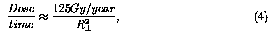
where  is the radius of the cylinder in cm and
1Gy=100Rad. This is a factor of 3000 less than at the SSC
and should not cause a serious problem if radiation hard electronics are used.
For example, tests with the CDF SVX-I detector11, without radiation hard
electronics, showed a doubling of the electronic noise for a dose of 20Krad. At
RHIC, a dose of 350Rad per "RHIC year" would be expected --- far
below this limit. Therefore, radiation damage should not be a problem at RHIC.
Neutral particles and the presence of a magnetic field around the vertex could
increase this dose, but the estimate suggests that it will not be important.
is the radius of the cylinder in cm and
1Gy=100Rad. This is a factor of 3000 less than at the SSC
and should not cause a serious problem if radiation hard electronics are used.
For example, tests with the CDF SVX-I detector11, without radiation hard
electronics, showed a doubling of the electronic noise for a dose of 20Krad. At
RHIC, a dose of 350Rad per "RHIC year" would be expected --- far
below this limit. Therefore, radiation damage should not be a problem at RHIC.
Neutral particles and the presence of a magnetic field around the vertex could
increase this dose, but the estimate suggests that it will not be important.