|

|

|

|
Tests of discriminator in MCM
Sangkoo Hahn and John Sullivan
The tests described in this document all used MCM serial number 117. This is a "grade B" MCM. It is not grade A because the AMU MUX's do not work.
In earlier work, Sangkoo Hahn had found that 4fC of charge injection (1 mip) resulted in a "step" in the preamplifier output of 60 mV. We use this result to translate signals seen on the spy line to mips.
This set of tests was done with the "bench calibration" on the TGV chip. The size of the charge injected is controlled by the Vcal DAC on each TGV chip. All scope traces were collected with 20 MHz bandwidth.
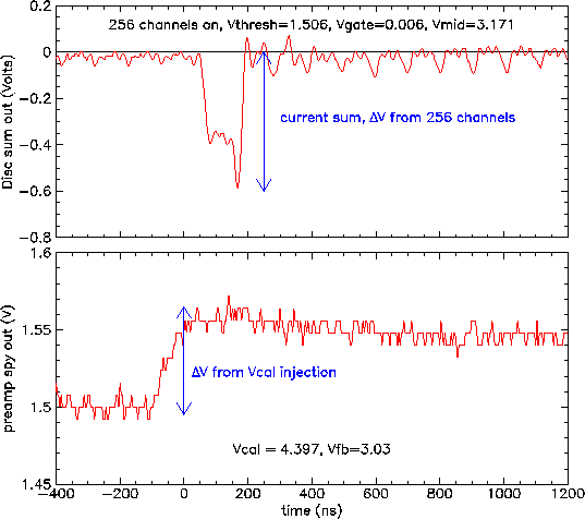
The following pair of plots show examples of a typical discriminator output signals with all 256 channels "on" (top) and a typical spy channel output for a single TGV preamp channel. This pair of plots was not taken in the same scope trigger. The top plot was taken with values we used in the past for discriminator settings -- in particular Vgate=0.006 (the lowest setting) and Vthresh was set about as low as we could set it without going into the noise (but there are some noise pulses). The big negative-going peak is the output signal. The "step" in the preamp spy output is about 72 mV -- a little more than the 60mV step expected for 1 mip. The step, followed by a slow decay (whose time constant is controlled by the Vfb DAC), is a typical signal from these preamps.
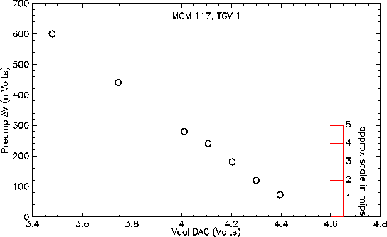
For the first TGV chip on MCM#117, we looked at the size of the "step" as a function of the Vcal DAC setting. This is shown in the following plot:
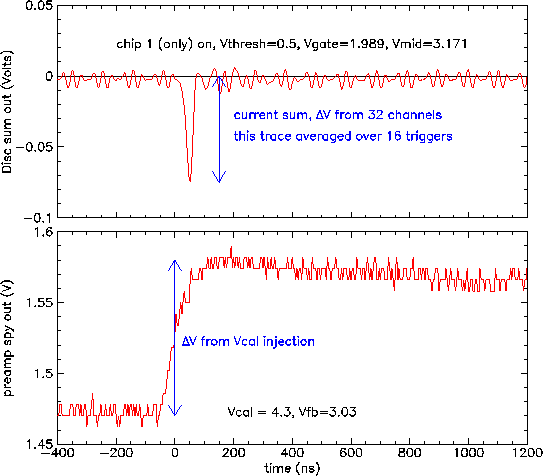
Following Chuck Britton's suggestion in a phone conference (September 16th??), we changed Vgate from 0.006 (used in the plots above) to 2.0V (actually 1.989V) and tried to adjust the threshold for each TGV chip individually. The following plot shows some scope traces for the discriminator sum output (top) and the preamp spy line for one TGV channel. Only the first TGV chip is "on" in this case. To be more specific, we used Vcal=4.3, Vfb=3.03, Vthresh=0.5, Vgate=1.989, Vmid=3.171, with all 32 CAL_ENABLE bits = 1 for the first TGV chip. For the other 7 TGV chips we used the same DAC settings except all CAL_ENABLE bits = 0 and all Vthresh=0.0. In the plot below, we put the scope in averaging mode for the current sum output -- it is the average of 16 consecutive scope triggers. All other plots on this page are from single scope triggers, without averaging.
The following set of 12 plots show the current sum output with all DACs set as in the plots above (i.e. TGV 1 "on", TGV 2-8 "off") except the values of Vthresh are changed in steps from 0.0 (highest discriminator threshold) to 1.8 (lowest threshold tested). At the highest DAC values, the injected charge (108mV on spy line, or a little less than 2 mips) is below the discriminator threshold and no output is seen. At a Vthresh DAC values 0.4 and above, the injected charge is above the threshold and an output signal is seen. The output pulse gets wider with a slightly smaller peak voltage as the Vthresh value is increased (discriminator threshold decreased). At Vthresh=1.6, a singificant increase in noise is seen. At Vthresh=1.8, the discriminator seems to be "on" continuously -- there is an offset voltage and no obvious response to the injected change.
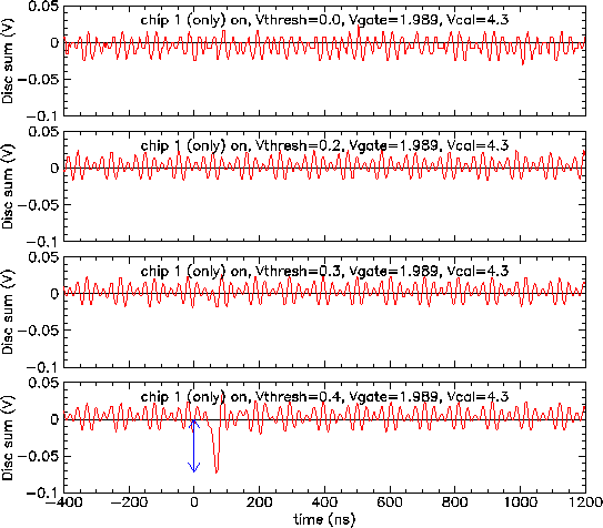
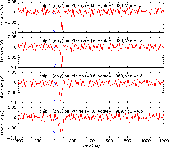
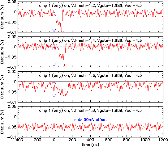
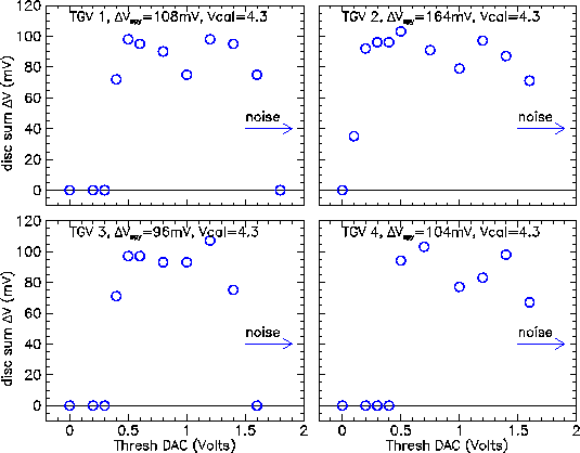
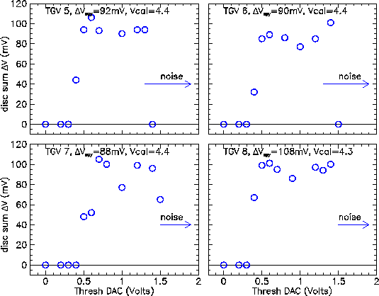
The following table summarizes the results from the plots above. The "threshold value" is the minimum DAC setting which allows the discriminator to fire. The "noise level" shows were the discriminator gets into the noise.
| TGV # | dV TGV spy (mV) | theshold value (Vthresh Volts) | noise level (Vthresh Volts) 1
| 108
| 0.5
| 1.5
| 2
| 164
| 0.2
| 1.5
| 3
| 104
| 0.5
| 1.5
| 4
| 108
| 0.5
| 1.5
| 5
| 92
| 0.5
| 1.3
| 6
| 90
| 0.5
| 1.3
| 7
| 88
| 0.7
| 1.5
| 8
| 108
| 0.5
| 1.5
| |
In later tests, for which we did not save any plots, we were able to get the discriminator on the first TGV chip to fire on a charge injection corresponding to 24mV on the preamp spy line output. Using 60 mV/mip, this translates to 0.4 mips. Due to the granularity of the Vcal DAC (the smallest steps are about 12 mV), it is hard for us to get much lower than this in our tests. At this level, the discriminator was able to trigger on the signal without triggering on most noise.
The discriminator still has one serious noise problem. For a period of 4.5 microseconds around the time of the ADC digitization, the discriminator is continuously on. This is true even if we set the Vthresh DACs to 0 Volts (the highest possible theshold, corresponding to at least 2 or 3 mips) with Vgate=2.0V. The first plot below shows the discriminator sum output -- the -0.45 V output level corresponds to all or almost all channels on the MCM firing simultaneously. The second plot shows the ADC_CLK_ENABLE line. The output from the current sum starts 0.6 microsec before ADC_CLK_ENABLE and stops 3.9 microsec after the leading edge of ADC_CLK_ENABLE (about 9.5 microseconds before the end of ADC_CLK_ENABLE). The third plot below shows the spy line output from one preamp channel. The discriminator seems to respond to a some charge which gets injected into the preamp at this time. The preamp output should be a slowly falling signal as is seen in the first 10 microseconds of the plot. Since the digitization occurs about 40 microseconds after the charge injection, the "real" step in the preamp spy line output occurs at about -40 microseconds -- which is not on the plot below.
