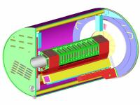
which is summarized below.
While going through the circuit summarized here:
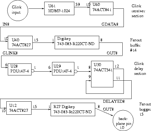
The duty factor gradually gets worse, going from this at the beginning:
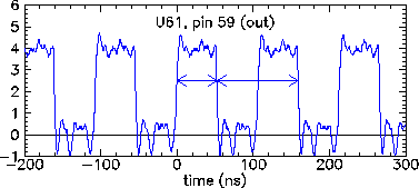
| At U61, pin 59, HDMP-1024 output, in G-link receiver block
|
to this at the end:
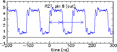
| At R27, pin 8, Digikey 743-083-RT220CT-ND output, in fanout buffer 15 block
|
This last signal goes on the backplane to the DCIM.
Looking at the same clock when it gets to the DCIM (
look here for the original report) we see (at U80, pin 2) on the bottom half of
the following pair of plots:
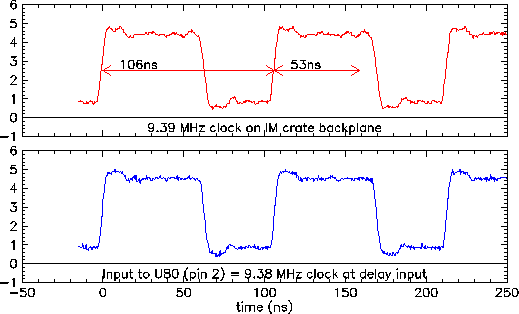
The "20 MHz" clock does not look
very good. The exact details of its shape depend on the
setting of a jumper (JP24) which adjusts the delay of the twp
10 MHz clocks in the XOR. The top plot shows the 20 MHz clock at the output of
U79, pin 8 (an XOR, 74ACT88) on the DCIM board. All of the
other 20 MHz and 40 MHz clocks on the board descend
from this clock. The input to this is the "10 MHz" clock (above),
which is delayed and then "XOR'ed" in this chip.
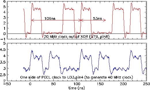
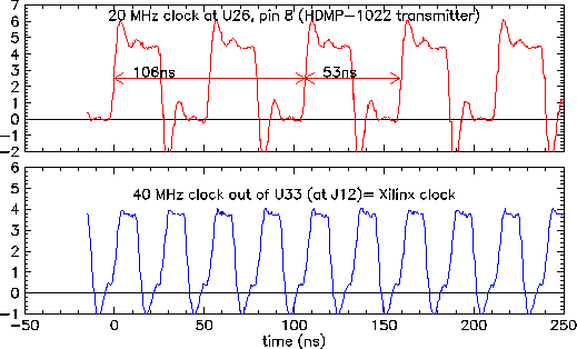
This 20 MHz clock is then used to make a 40 MHz clock, which
the Xilinx FPGA then scales down to make the 20 MHz clock
(my original report had this detail wrong):.
These clocks do not looks a ugly:
Look herefor a summary of DCIM test results.
The colums labeled 1...6 say whether each of the 6 output channels worked
(=1) or now (=0). It is interesting that the top Glink is most likely
to fail (channel 1-2).
Look here for table summarizing
which channels are currently being read out. It includes notes saying which are
not read out due to Glink problems.
Other possibly relevant notes:
Here is an old note (4-Oct-2000) about DCIM problems.
Here is another old note (14-Nov-2000) about DCIM problems.
updated 3-Aug-2000
John Sullivan