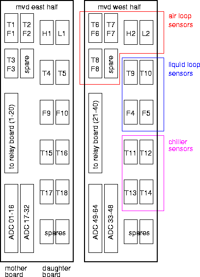
These 'sensor distribution module' are double-wide 6U VME boards, with front
panel assignment as indicated. The sensor names (Tx, Fx, Hx) correspond to the
nomenclature on
this schematic of the cooling systems.
T1-F5 belong to the East half, and T6-F10 to the West half of the MVD. T11-T18
monitor temperatures at the chillers.
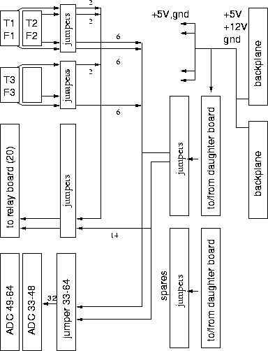
The left half of the connectors sit on a main board which plugs into the VME backplane, and the right-hand half of the connectors sits on a daughter board. All connectors are 3M 'condo' connectors, double-high 0.1" pin spacing, 3-wall. The sensor connectors are 2x10 and 2x14 pins, the ADC connectors are 2x34 pins. The relay board connector is a single-high 26-pin connector.
|
The main board gets power from both VME backplane connectors. The sensors on
this level are the TxFx sensors, plus one spare. Signals also arrive from the
daughter board. A subset of all these signals these are routed to the ADC's,
and some are also routed to the relay board.
All incoming and outgoing lines go through jumper blocks, where initially all lines are jumpered straight through. Anny signal can be re-routed if necessary.
The details are in the 'netlist' below and in the layout of the PC boards | . |
Here is the VME backplane, J1-top, J2=bottom.
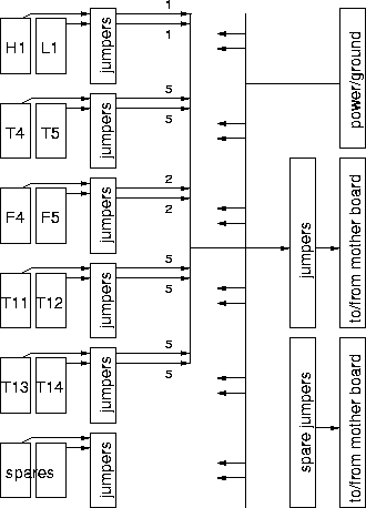
All sensors signals from this level are sent down to the main board. Power
comes up from there.
A more detailed schematic of this daughter board, Here are the PC boards |
'Net List' |
---|
-------------- MAIN BOARD ----------- from pin to ADC relay sensor # chan(pin) chan(pin) ------------------------------------ T1F1 1 power +5 . . 2 ground 3 power . . 4 ground 5 power . . 6 ground 7 low-low . . 8 low 9 high 1(2) 10 high-high 2(4) 1(1) 11 analog 3(6) 12 - 13 low flow 4(8) 4(7) 14 high flow 5(10) T2F2 1 power +5 . . 2 ground 3 power . . 4 ground 5 power . . 6 ground 7 low-low . . 8 low 9 high 6(12) 10 high-high 7(14) 2(3) 11 analog 8(16) 12 - 13 low flow 9(18) 5(9) 14 high flow 10(20) T3F3 1 power +5 . . 2 ground 3 power . . 4 ground 5 power . . 6 ground 7 low-low . . 8 low 9 high 11(22) 10 high-high 12(24) 3(5) 11 analog 1(26) 12 - 13 low flow 14(28) 6(11) 14 high flow 15(30) spare 1 power +5 . . 2 ground 3 power . . 4 ground 5 power . . 6 ground 7 low-low . . 8 low 9 high . . 10 high-high 11 analog . . 12 - 13 low flow . . 14 high flow --------- DAUGHTER BOARD ------------ from pin to ADC relay sensor # channel channel ------------------------------------- H1 1 power +5 . . 2 ground 3 analog hum 17(2) . 4 - 5 - . . 6 - 7 - . . 8 - 9 - . . 10 - L1 1 power +12 . . 2 ground 3 level 18(4) . 4 - 5 - . . 6 - 7 - . . 8 - 9 - . . 10 - T4 1 power +5 . . 2 ground 3 low-low . . 4 low 5 high 19(6) 6 high-high 20(8) 7(13) 7 analog temp 21(10) 8 - 9 - . . 10 - T5 1 power +5 . . 2 ground 3 low-low . . 4 low 5 high 22(12) 6 high-high 23(14) 8(15) 7 analog temp 24(16) 8 - 9 - . . 10 - F4 1 power +12 . . 2 ground 3 low flow 25(18) 9(17) 4 analog 26(20) 5 - 6 - . . 7 - 8 - . . 9 - 10 - . . F5 1 power +12 . . 2 ground 3 low flow 27(22) 10(19) 4 analog 28(24) 5 - 6 - . . 7 - 8 - . . 9 - 10 - . . T11 1 power +5 . . 2 ground 3 low-low . . 4 low 5 high . . 6 high-high 7 analog 29(26) 8 - 9 - . . 10 - T12 1 power +5 . . 2 ground 3 low-low . . 4 low 5 high . . 6 high-high 7 analog 30(28) 8 - 9 - . . 10 - T13 1 power +5 . . 2 ground 3 low-low . . 4 low 5 high . . 6 high-high 7 analog 31(30) 8 - 9 - . . 10 - T14 1 power +5 . . 2 ground 3 low-low . . 4 low 5 high . . 6 high-high 7 analog 32(32) 8 - 9 - . . 10 - --------- BY ADC CHANNEL ------------ signal, ADC relay pin chan(pin) chan(pin) ------------------------------------- T1 9 high 1(2) T1 10 high-high 2(4) 1(1) T1 11 analog temp 3(6) F1 13 low 4(8) 4(7) F1 14 high 5(10) T2 9 high 6(12) T2 10 high-high 7(14) 2(3) T2 11 analog temp 8(16) F2 13 low 9(18) 5(9) F2 14 high 10(20) T3 9 high 11(22) T3 10 high-high 12(24) 3(5) T3 11 analog temp 13(26) F3 13 low 14(28) 6(11) F3 14 high 15(30) H1 3 analog 17(2) L1 3 analog 18(4) T4 5 high 19(6) T4 6 high-high 20(8) 7(13) T4 7 analog 21(10) T5 5 high 22(12) T5 6 high-high 23(14) 8(15) T5 7 analog 24(16) F4 3 low 25(18) 9(17) F4 4 analog 26(20) F5 3 low 27(22) 10(19) F5 4 analog 28(24) T11 7 analog 29(26) T12 7 analog 30(28) T13 7 analog 31(30) T14 7 analog 32(32) --------- BY RELAY CHANNEL ----------- signal, ADC relay pin chan(pin) chan(pin) -------------------------------------- T1 10 high-high 2(4) 1(1) T2 10 high-high 7(14) 2(3) T3 10 high-high 12(24) 3(5) F1 13 low 4(8) 4(7) F2 13 low 9(18) 5(9) F3 13 low 14(28) 6(11) T4 6 high-high 20(8) 7(13) T5 6 high-high 23(14) 8(15) F4 3 low 25(18) 9(17) F5 3 low 27(22) 10(19) ----------- VME BACKPLANE ----------- a b c -------------------- J1 9 GND . GND (top) 11 GND . . 15 GND . . 17 GND . . 19 GND . . 31 -12 . +12 32 +5 +5 +5 -------------------- J2 1 . +5 . (bot) 2 . GND . 12 . GND . 13 . +5 . 22 . GND . 31 . GND . 32 . +5 . -------------------------------------- |