David Jaffe, Mike Bennett, Sangkoo Hahn, and Larry Marek.
Los Alamos National Laboratory
PHENIX-MVD-99-6, PHENIX Note 377
I. Introduction
This note documents the procedures, equipment, and specifications used in the characterization and evaluation of silicon double-metal pad detectors for use in the PHENIX Multiplicity Vertex Detector. Storage of detector data in the internet accessible database is covered in Appendix B. This note does not document the use of the laser station or the evaluation of any part of the FEE.
II. Detector Specifications
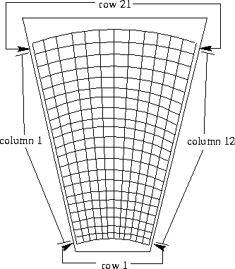
The specifications submitted to Micron Semiconductor call for PIN type, AC-coupled, single-sided, polysilicon biased, double-metal pad detectors with 252 active pads arranged in 12 columns of 21 rows each. A complete listing of the physical and electrical specifications for these detectors can be found in Appendix A.
Depending on how well they meet these specifications, all detectors are given a grade of A, B, or J. An "A" grade detector passes all specifications and is suitable for use in the operational MVD. A "B" grade detector meets most specifications and is suitable for use as a spare, or in tests of other components requiring an operable detector. Only detectors that meets nearly all specs, but have 4 or 5 bad channels, are assigned B grades. A "J" grade detector is suitable for mechanical tests only.
III. QA Testing Overview
To test these specifications and assign grades, we have devised the following series of tests to be executed in the order listed. With pad detectors, unlike strip detectors, all tests are completed for all detectors regardless of performance on previous tests. Even if a detector badly fails one of the first tests, all subsequent tests are carried out to provide data on the manufacturing process. Additionally, failed detectors may be used as spares, necessitating complete test data for all detectors.
When received from Micron Semiconductor, the detectors each come in ~5 inch square plastic cases labeled with the detector's serial number and type. In addition each detector comes with its associated test structures packaged separately in a similar case with the same serial number as its corresponding detector and the label "test structures". As the detectors themselves have no identification on them, it is important to keep them associated with their correct serial numbers via labels on either their original shipping boxes, or their mounts. Detector mounting will be discussed in detail later in this document. Upon receiving, the initial database records are created for each detector. See Appendix B for details.
As temperature and humidity can affect the electrical characteristics of silicon devices, the specifications require that all measurements be made at 21 deg. C (± 3) and at a relative humidity of less than 50%. This may require that the detectors and test structures be acclimatized in a controlled environment for a certain time before testing. Ordinarily this will not be necessary as the clean-tent, where all tests will be performed, is usually within the temperature and humidity ranges specified.
All software related to these test are located on the main silicon test Macintosh Quadra 610 in the clean tent, in the "Macintosh HD:Silicon Detector testing:" subdirectory. The only exception is for the detector burn-in test. See section IX for details.
The data produced in these tests are stored in three separate places. First, as each test is performed, the relevant data are entered into the Silicon Pad Detector Database. This is an internet accessible database located at BNL. Appendix B details its use and location. Second, all data files are stored on the Macintosh Quadra 610 in the clean-tent for eventual burning onto CD-ROM using the "CD Burner" application. All LabVIEW produced data files are comma-delimited text files, readable by most spreadsheet programs. Lastly, printouts of all data files or graphs are stored indexed by serial number in the white three-ring binders on the bookshelves in the back of the clean-tent. Each of the following test descriptions specify exactly what data to store where and in what form for each individual test.
The following test descriptions are listed in the order performed and specify the equipment used, output data formats and storage locations, and the specifications addressed. Schematic diagrams and illustrations are included where needed. This sequence of tests, when completed, will generate all data needed for detector final evaluation and grade assignment.
IV. Test Resistor Measurement
Requires the use of Ohmmeter and a probe station.
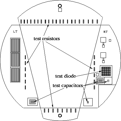
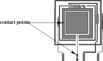
The first test performed is the resistance measurement of a subset of 16 out of a total of 41 polysilicon test resistors included in the test structures for each detector. These test resistors reside on all four pieces of silicon illustrated in figure 1. Typically every other resister is measured on the left, right, and bottom pieces, along with 6 more spread out on the top piece, for a total of 16.
The test piece should be manipulated only with a vacuum pen, and placed directly on the vacuum chuck of the probe station, using the vacuum to hold it in place. The measurement is performed using two probes, set down on the contact pads at each end of each test resistor, connected straight to a multimeter in resistance mode. The resistor numbers and values, along with the date, time, temperature, humidity, and names of those performing the test are recorded on a "T Resistor worksheet" (an Excel document stored with the VIs on the Macintosh Quadra 610 in the clean tent) and entered in the database (see appendix B for details on database entry). The completed "T Resistor worksheets" are stored in the binders.
V. Detector Thickness
VI. Test Diode Capacitance vs. Bias Measurement
Data taken from 2-60V at 1MHz test frequency (defaults programmed into VI).
The next test is a measurement of the test diode capacitance as a function of bias voltage. This gives us an indication of the depletion voltage of the detector. The test diode is the large waffle structure shown in figure 1. Unlike the test resistors, the test diode must be tested in complete darkness to eliminate photoelectric effects.
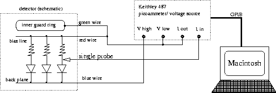
To set up for this test, the test piece is mounted on the vacuum chuck. Two probes are used to make the electrical connections to the backplane and the top of the test diode. Since the test diode is so large, the tips of these probes should be inverted so as to use the bend as the contact point and preserve the points for other tests that require the precision afforded by the probe tips. These probes are connected to a special box within the RF black box enclosure that combines the two bias lines with the four measurement lines from the HP 4284A Precision LCR meter (see figure 2 for a schematic diagram). The backplane (via the chuck) is connected to the box terminal labeled "HV" and the top of the diode is connected to the box ground terminal. The voltage source of the Keithley 487 is connected to the BNC connector on the bottom of the box (outer = ground). The HP 4284A makes the capacitance measurements.
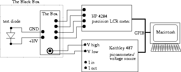
Both instruments, and the measurement run, are controlled by a LabVIEW Virtual Instrument (VI) running on a Macintosh computer via GPIB connections. The VI is called "single C-V.vi" and is located in the directory "Macintosh HD:Silicon Detector Testing". To run the VI, the user must first set a few input variables. The first is labeled "Detector Description". Generally the serial number of the tested detector is entered here. Whatever character string is entered in this control, e.g. "123", will be concatenated with "_CV.txt" to create the data file "123_CV.txt" in the "detector data" sub directory. Next the user decides whether the data file should be appended to or overwritten by toggling the "Data" button. There is generally no reason to append to these files, so overwrite is the default. The VI has one default test frequency of 1 MHz since the database is formatted to accept only datafiles with a single test frequency. If the user wishes to use another or multiple test frequencies, these must be entered in the "test frequency" control. Lastly the "Max. Bias" control must be set to the appropriate value (default is 60V). There is also a spy function that allows the user to monitor the CV data of one test frequency as it is measured. To do so, simply set the "spy freq." control to whichever test frequency you wish to monitor. At this point the VI is ready to run. In running, the VI increments the bias voltage in one volt steps, stopping at every second voltage to take measurements. At each measurement voltage, the VI cycles through the test frequencies, taking capacitance measurements for each, and storing the data in a two dimensional array. Once the maximum voltage is reached, the VI automatically ramps the bias back down to zero, writes out the data file, and beeps to inform the user that the run has completed.
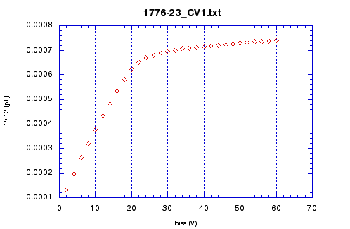
Once the data is taken, a graph is made of bias voltage vs. 1/capacitance2 and printed for storage in the binders. See figure 3 for an example. The calculations for this can be done with either Excel, or Kaleidagraph, but the raw data files must be kept unchanged to facilitate automatic loading into the database. This graph should rise steeply and then level off suddenly. The depletion voltage is the first voltage just past the transition "knee". For this graph the depletion voltage is 24V. The raw data file is burned onto CD-ROM and entered into the database along with the date, time, temperature, humidity, and names of those performing the test (see appendix B for details).
VII. Coupling Capacitor Breakdown Voltage
Requires the use of Keithley 487 picoammeter/voltage
source, black box probe station.
Performed on one detector at a time.
Failure rejects detector and stops testing.
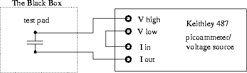
Measurement of the coupling capacitor breakdown voltages are made on any one of the test pads. In this test, the voltage source and ammeter are connected in series with the coupling capacitor as illustrated in figures 4 and 5. Since the device is a capacitor, it should pass no current until the silicon dioxide dielectric breaks down and essentially shorts out the capacitor. This will be marked by a sudden current of hundreds of µAmps or more. The specifications call for a breakdown voltage of >70V, but in testing many detectors, we have yet to see one test capacitor that breaks down at less than 100 Volts. So it has been decided to save time by testing only one capacitor to 100 volts bias. The wafer's performance should be consistent enough across its face to ensure that if one test pad breaks down at >100V, none of the pads, either on the test pieces or on the detector, will break down at less then the specified 70V. Once a pad has broken down, the capacitive coupling is permanently destroyed, rendering it useless for any other testing. This measurement is made in the Black Box as a precaution; incident light may or may not affect it significantly. The data are recorded on "T Capacitor worksheet" and then entered into the database along with the date, time, temperature, humidity, and names of those performing the test (see appendix B for details).
VIII. Mounting
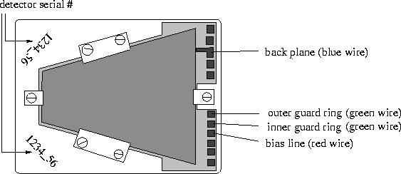
At this point, all surviving detectors, i.e. those whose test structures have passed all of the preceding tests, are mounted for final testing of the detectors themselves. The detector mounts consist of an aluminum plate approx. 4 x 3 x 1/4 inches. On the top surface of the plate is a shallow relief that receives a copper coated G10 board. Located on all sides of this pc board are Teflon clamps that hold the detector and the pc board firmly to the aluminum base plate. The copper on the G10 board is cut away into several separate traces for the backplane, bias ring, and inner and outer guard rings of the detectors. On one end of these traces are large pads for soldering to color coded lead wires for connection to multimeters, voltage sources etc. The three leads are: Red = bias line, Blue = back plane, Green = inner and outer guard rings. The other ends (except for the backplane trace) stop just short of the edge of the detector and are connected to their proper detector structures via gold wire bonds. The backplane trace is connected directly to the detector backplane Note: no indium is used for mounting pad detectors. Both the aluminum plate and the G10 board have 0.5 inch diameter holes in the center to hold an alpha source for depletion testing. In order to keep track of the detector's identification, it is necessary to write the detector's serial number on the jig in pencil (soft lead #1 works best). Once mounted, the detectors are sent off to be wire bonded. The bias line and inner both guard rings will be wire bonded since the outer guard ring is needed to test for shorts between the two metalizations. Figure 6 illustrates a mounted detector. Once bonded the detectors are ready for burn-in and final testing.
IX. Burn-in, Total Pad & Inner Guard Ring Leakage Current Measurements.
After mounting, the detectors are burned-in by the application of 50V reverse bias for at least 72 hours to eliminate transient electrical effects caused by the detectors response to sustained bias. During this time they are also allowed to acclimatize to the temperature and humidity environment required by the specifications for the remaining tests. This burn-in will take place in the Burn-in Box to eliminate photocurrents, and can be performed on up to 10 detectors at a time, automated by the Macintosh. Some of the hardware can handle up to 17 detectors, but using the Keithley 7011 scanner switch card has cut this down to 10.
To set up for the burn-in process, the detectors are placed on a pigeonhole/shelf in the burn-in box. Each detector slot has a label from 1 - 17 that corresponds to a bundle of cables that connect each detector to the bias supply. Each bundle has three color coded wires: red - for the bias line, blue - for the backplane, and green - for the inner guard ring. Each of these wires ends in a micro-clip connector of the same color except for the green inner guard ring line which has a black connector (the supplier was out of green). These are clipped to their proper detector leads which, coincidentally, have the same color code scheme (see figure 6). A list must be made identifying which detector serial number goes with which burn-in slot (1-10); this will be entered into the VI to identify which data goes with which detector. The burn-in box is then closed and sealed with blackout tape to ensure total darkness.
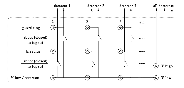
Figure 7 is a schematic diagram of the switch board, located on one side of the Burn-in Box. The front has a total of 18 subsections: 1 set of connectors and switches per detector (17), plus the last section on the right containing the "V low" and "V high" Lemo connectors. Each detector subsection contains three Lemo connectors, and two single-pole-single-throw switches. Each of the two input Lemos (labeled "guard ring" and "bias line") are connected to the "V low / common" Lemo through a shunt switch. For the burn-in a Keithley 487 voltage source will be plugged into the "V high" and "V low" terminals to provide bias voltage, and all switches will be set to "shunt".
Figure 8 is a schematic diagram showing the complete setup for the burn-in process. Each guard ring and bias line lemo is connected to the input terminals of the Keithley 7002 switch system via a Keithley 96 channel cable and a custom lemo converter board. The inner guard ring lemos for detectors 1-10 are connected to switch channels 1-10 (IGR signal) and 11-20 (IGR shunt). The bias line lemos for detectors 1-10 are connected to switch channels 21-30 (bias signal) and 31-40 (bias shunt). As of now, the switches are all left in the "in"(open) position for burn-in and are not changed. The switch board was designed before the process was automated using the Keithley 7002 to switch between detectors and measurements, so the switches are now vestigial features as are the common/low/ground lemos.
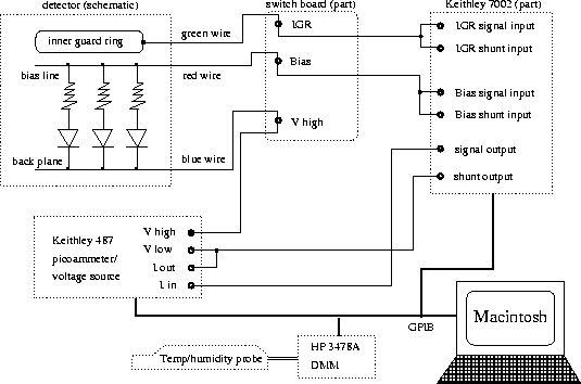
Each measured channel (inner guard ring and bias line) for each detector is connected to two inputs on the Keithley 7011 scanner cards in the 7002 switching mainframe. This shorting occurs on a small adapter board that connects the lemo outputs of the Burn-in Box to the 96 pin connector of the Keithley 7011 connector cable. Additionally, this board has two labeled terminals for the signal in (labeled "signal") and signal out (labeled with a ground symbol) alligator clips of the Keithley 487 voltage source/picoammeter. This shorting allows the current meter to be switched in and out of each circuit without breaking the bias path even momentarily. When switching from one measurement to another, first the structure to be measured is switched in, creating a momentary double current path, and then it's shunt switch is opened, leaving only the patch through the current meter. In this way, the bias supply to each detector structure is never broken. The Keithley 7002 and 487 are controlled by the VI on the Macintosh via GPIB cables. Temperature and humidity data are read by a temperature/humidity probe translated by the HP 3478A multimeter and readout via GPIB.
The burn-in process and simultaneous measurement of inner guard ring and total pad leakage currents are controlled by the VI "burn-in(7011).vi.3.1" located on the burn-in control Macintosh Quadra 700, in the "Macintosh HD:LabVIEW 3:Silicon Detector Testing" subdirectory. Initialization proceeds as follows. The "Burn-in voltage" control is set to the desired voltage or left at the default 50V. The "Measurement Interval" (time between measurements) defaults to 1 hour. This VI has a excess current cut-off feature that can be turned on or off by the "Excess Current Cut-off" button. Additionally the cut off level can be set by the "Current Cut-off level (µA)" control. Should the cut-off engage, the bias voltage goes to zero, the "VI shutdown" light turns red, and execution of the VI stops. Since this VI writes the data out to files after every measurement, all data taken previous to the shut-down is saved to the data files described in the next paragraph. Lastly, and most importantly, the detector serial numbers must be entered in the "Detectors Present" control box. If detector 1234-56 is hooked up to slot 5, then "1234-56" must be entered in window 5 of the "Detectors Present" control box. Between 1 and 10 detectors may be burned in at a time, but it is crucial to the execution of the VI that they be connected and entered into slot 1 through X with no gaps. Once the burn-in is started, detectors can be removed from the measurement list by deleting their serial numbers from their proper "Detectors Present" window. In this case, the number "-777" will be substituted for a current measurement in the data files. Lastly, there are two chart displays for monitoring the leakage currents of whichever detector slot is selected by the "Spy Detector Number" control. The VI is now ready to execute.
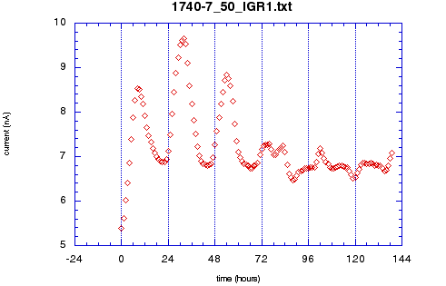
When started, the VI checks for detectors present, ramps the bias voltage to the user specified level, and takes the first measurements of temperature and leakage current. Just before the first measurements are taken, approximately 1 minute from go, the VI creates two files for each detector present, one for the inner guard ring data and another for the total pad data. The file names are the detector serial numbers concatenated with either "_IGR1.txt" or _strips1.txt", and are located in the directory listed in the "Data Files Directory" window. This VI was originally written for use with strip detectors, hence the "_strips1.txt" suffix. The fact that the data are of course total pad leakage currents and not total strip isn't critical. If no detectors are present an error window appears and execution stops. Each file contains a comma delimited spreadsheet/text file with four columns and a line of column headers: sequence #(something the database needs), time (hours since start), temperature (F), and current (nA). After one measurement interval, another set of measurements is made, the files opened, the new data appended, and the files closed again. The VI then waits for another measurement interval, and repeats the process. This will go on indefinitely until the user terminates execution by hitting the "Execution" stop button. During the interval between measurements, the VI checks every minute to see if the user has terminated execution. If not, it proceeds normally. If so, it ramps the voltage down to zero and beeps. The termination process takes a total of 1-2 minutes. Direct termination of the VI using the LabVIEW stop button has no adverse affects save that the user must ramp down the voltage manually.
The data is then plotted in Kaleidagraph; see figure 9 for an example. The periodic variation is due to temperature fluctuations during the 6 days of measurement. In this case the measured currents are far below the 1.5µA specification, and so pass easily. Sometimes the variation actually straddles the specification, in which case the decision is a bit subjective. If the trend appears to be stable, or even decreasing, the detector meets specifications. If the general trend is increasing, it fails. The plots stored in the binders, the raw data files saved on CD-ROM and entered into the database along with the date, time, temperature, humidity, and names of those performing the test (see appendix B for details).
X. Readout Trace Capacitance
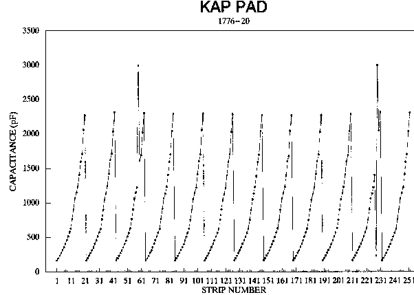
Each pad detector comes with a graph of capacitance vs. pad# from a test performed by Micron as part of their in-house QA procedure. Figure 10 is a scan of one of these graphs. A broken readout trace will show up as a low capacitance spike in the normal semi-parabolic curve of measurements of one column. All suspect spikes will be confirmed by making a similar capacitance measurement using the Alessi single probes. Any channel showing low capacitance in both measurements is considered a bad channel and is marked as such on the Micron plot, and entered in the database. See Appendix B for details. Readout traces shorted to their neighboring traces, the bias line, or the guard rings will usually show up as a high capacitance spike. Unfortunately this is not totally reliable, and so the following resistance test must be performed before all shorted traces can be found.
XI. Readout Trace Resistance (shorts)
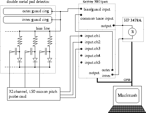
Shorts in the readout traces will also usually show up in the previous capacitance measurements, but not always. So an additional resistance measurement is required. Using the 150µm pitch probe card and the Keithley 7002 Switching Mainframe, resistance measurements are made between each readout trace and its neighbors, the bias line, and the guard rings.

This measurement is very similar to the individual strip leakage current measurement made of the strip detectors in that essentially you are selecting one channel at a time and making a measurement using a probe card and the 7002 switch box. The key differences are that here the 7002 is configured to serve as two separate switch systems, and that for each channel selected, two measurements are made. First, the resistance between the selected channel and all neighboring channels contacted by the probe card is measured, and then that between the selected channel and the bias and guard ring structures. See figure 12 for a schematic diagram of the measurement setup. The 7002, as used here, has 5 Keithley 7158 low current scanner cards installed in the back. Each card has 10 input channels and two output channels. The double outputs allow the cards to be daisychained together to make multiple configurations. For this measurement, they are used to create 1 40 channel (4 card) switch system, and a separate 10 channel (1 card) system. In this way each half of the resistance measurement is controlled by the 7002 switch system.
An operational difference between this measurement and the individual strip leakage current measurement is that while the probe card has 32 pins, the pad detector geometry of 12 columns x 21 rows makes it logical to perform this test in increments of 21. The extra pins of the probe card allow for a resistance measurement between pins 21 and 22 while still moving the probe card 21 channels at a time. This is facilitated by the fact that every 21st readout bond pad is numbered. Note: pad 190 is mislabeled as 198. For most probe card setdowns, the pin one is set down on channels 1, 22, 43 etc. (conveniently labeled on the detector). Left justified if you will. This results in the last 10 pins being extraneous for most measurements. For the last letdown, the situation is reversed. The probe card is set down with pin 32 on the last channel, 252, or right justified. This protects the wirebonds for the guard rings and bias line which lie nearby (see figure 11). The VI that runs this measurement automatically adjusts it's scan pattern to account for this.
Operation of the "pad-shorts.vi" VI is straight forward. Upon starting, the serial number of the detector to be tested is entered in the "Detector ID#" field. Whatever character string is entered here will be concatenated with "_shorts1.txt" to create the name of the produced data file which will automatically be stored in the "pad data" subdirectory. The full path name will appear in the "Data File:" window at the bottom of the screen. The "Channel Range:" control must be set to the properly for each run to ensure correct channel numbering in the data file. Also, this control tells the VI which switch scan pattern to follow. The last two controls are the "Common trace Channel #:" and the "Bias/Guard Line Channel #:". These are set to default values of 41 and 42 respectively and need only be changed if the user wires these inputs to different switch channels in the Keithley 7002 switch mainframe. At this point the VI is ready to execute.
There are two waveform charts in this VI, "Trace - Bias/Guard Resistance (Ohms):", and "Trace - Trace Resistance (Ohms):". Each displays the measured voltage for each channel relative to the respective structures. Good channels will return measurements off the scale, in which case the number returned by the HP 3478A is 9.99999E9. Shorted channels return resistances anywhere from 1 to 100 KOhms typically. Each chart has vertical bars every 21 data points to help the user keep track the measurements.
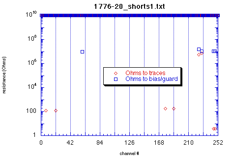
Any significant low resistance spike (<100MOhms)(see figure 13) is a suspected short. Suspected shorts are later confirmed using the Alessi single probes. Neither the capacitance nor the resistance measurements are perfectly reliable in detecting shorted traces, so data from these two resistance measurements, and the previous two capacitance measurements are pooled together. A channel showing faulty behavior in any two of these four measurements is considered a bad channel and marked as such on the Micron plot, and on the resistance plot, and is entered in the database. See Appendix B for details.
XII. Individual Pad Leakage Current
Performed on 1 detectors at a time.
The last and most time consuming test performed on the pad detectors is the measurement of leakage currents through individual pads at various bias voltages. Due to the geometry of pad detectors, it is not possible to use a probe card to automate the measurement of multiple channels. Instead we are forced to painstakingly test each and every pad with a single probe. The flip side is that the setup is fairly simple and the execution even simpler. Figure 14 is a schematic diagram of the measurement setup.
Since the readout bond pads are numbered sequentially across the top of the detector, it is logical to follow this order in testing the pads. This corresponds to starting with the pad at column 1, row 1, and moving up the column to column 1, row 2, etc., moving over to the next column as each is finished. See figure 15 for a diagram of the pad numbering scheme.
Once the probe is in position on the proper spy pad, the VI "single-pad.vi" runs the measurement. Initialization is similar to previous VIs. The serial number of the detector under test is entered in the "Enter Detector ID#:" control to be concatenated with the string "_1pad.txt". This becomes the name of the produced data file, the full pathname of which will be displayed in the "Spreadsheet file path/name:". Since this VI is used on pad detectors only, the data files are stored in the "pad data" subdirectory. The "Measurement Voltage Array:" control contains the test voltages to be used. The default values are 10, 20, 30, 40, 50, 60, and 70 Volts. The "Settling Delay (sec):" control is set for a default of 2 seconds delay before making a leakage current measurement at one of the test voltages. The "487 current range:" is set by default for the 200nA range. The "Present Voltage:" indicator is not a control and merely tells the user at what voltage level the detector is currently.
The remaining controls, "Row/Column Selection:", "Column #:", and "Row #:" are used to record the row and column number data for the measurements in the datafile. The "Row/Column Selection:" control default mode is set to "manual". In this mode, whatever values are entered in the "Column #:"(default 1) and "Row #:"(default 1) controls will be entered in the datafile. When "Row/Column Selection:" is set to "auto", the row and column numbers automatically advance themselves in the proper pattern, i.e., column 1 row 1, column 1 row 2, etc. From column X row 21, the VI advances to column X+1 row 1. In this way the VI follows the same pattern as the sequential readout bond pads on the top edge. It should be noted that the row and column numbers are advanced at the beginning of VI execution. Recommended operation is to make the first measurement, of C1 R1, in manual mode, and then for C1 R2 simply switch to auto mode. The VI will automatically switch the values to C1 R2 and then execute. These values are stored from one execution to the next so long as the VI is kept open. Closing the VI wipes out the values and reverts them to the LabVIEW default. This is why it is recommended to first run in manual mode to initialize these variables. It must also be noted that even in auto mode, the front panel control values take precedence over the stored variable value, so if sequentially the values should be C3 R3, but the user enters C4 R4, the VI will take the entered values, C4 R4, increment to C4 R5, and then execute. Using these controls properly, operation consists of simply moving the probe to the next spy pad, and starting the VI.
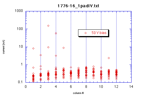
Once all pads are tested, two graphs of leakage current data is plotted by columns. See figure 16 for an example. Each column contains 21 data points, one per pad in the 21 rows. A separate graph must be made for the 50V and 70V data since there are differing specifications for each voltage. At 50V, any channel drawing more than 10nA is considered bad (high current). At 70V, any channel drawing more than 100nA is considered bad (low breakdown voltage). So in figure 16 we can see that there are two bad channels on this detector located in columns 3 and 4. The exact identity of these bad channels can be determined by looking in the raw data files. These bad channels are added to the set of bad channels determined by the Micron data, section X, and the shorts data from section XI to determine a total number of bad channels.
Unfortunately, the IV behavior of our detectors is not constant over time. Channels that showed excessive leakage currents upon initial testing, may show dramatic reductions several months later. Because of this it is necessary to retest the leakage currents of any high current channels on detectors that were failed because of excess bad channels. If the detector has too many bad channels (>3) due to shorts, breaks, or dead channels, it is not necessary to retest since the outcome cannot affect the final evaluation.
Appendix A: Detector Specifications, Physical and Electrical
Appendix B: The Pad Detector Database