Figue Fig.4
The strip detectors on the inner barrel and the outer barrel have very similar structure. The individual strip or pad currents in the respective strip or pad detectors are on the order of 1 nA. We require the individual strip or pad leakage currents in an acceptable detector to be lower than 10 nA. The characteristic of capacitance vs voltage of individual strips indicates a full depletion around 20 to 25 Volts, and the alpha-source test indicates a full depletion around 35 Volts. The leakage current in the outer guard ring is quite high, and the one in the inner guard ring is lower than 7 uA. The outer guard ring is floated during operation and the leakage current in the inner guard ring for an acceptable detector is required to be lower than 15 uA.
The C/V and alpha-source tests indicate a full depletion around 40 Volts. We require the depletion voltage for an acceptable detector as determined from 1/C^2 plot at 1 MHz to be lower than 35 Volts.
Figue Fig.5
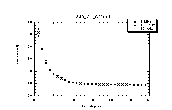
Figure 5: C/V test of depletion voltage.
The last figure of this poster shows the characteristic of individual strip currents vs voltage for a silicon detector with high interstrip resistance. We require the interstrip resistance for an acceptable detector to be larger than 100 MOhm.
Figue Fig.6
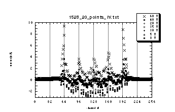
Figure 6: I/V responses in individual strip with low and high
interstrip resistance.
We use a beta-source stand to measure the additional cross talk in a pad detector induced by double metal design (see the poster in this section by Sangyeol Kim of Yonsei University, Korea). The measured cross talk is lower than 3%, which is acceptable for the performance requirement of the MVD endcaps.
 Next: Summary
 Previous: Silicon Pad Detectors