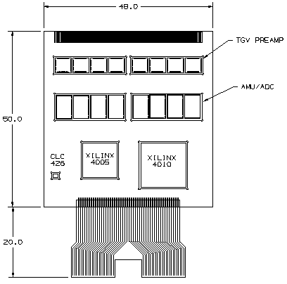
| The front-end electronics described on the previous slide will be implemented on multi-chip
modules (MCM's). A picture of a 256-channel module is shown on the left. It
consists of a 48x50x1 mm ceramic substrate, into which wells are milled that
hold the bare die (chips). The depth of the wells is such that the surfaces of
the die are level with the top surface of the substrate. In the figure, from
the top to the bottom, there are two wells holding four 32-channel preamps each,
below that two wells holding four 32-channel AMU's each, two wells for the Xilinx
FPGA's and one for an op-amp.
First a metal layer is deposited on the substrate, going into the wells. Then
the die are placed in the wells. Next, a film of Kapton is placed on top, and
a laser drills holes in this layer where contacts need to be made to the
chips. Next, a layer of traces is deposited on this, using standard
lithographic techniques. Another film of Kapton is placed over this, and the
process repeats a total of 4 times (analog signals, power distribution,
digital signals, ground planes). Finally, some surface-mount capacitors
are mounted on top.
|