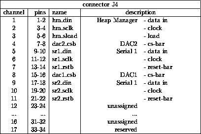
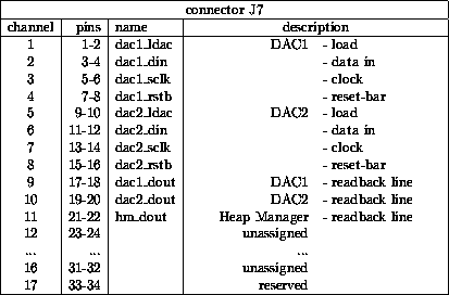
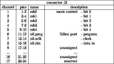
The pin assignments are described in the tables below. During the test, the
communications ports on the LeCroy 2366 were all configured as output ports.
Since lines 9-11 on J7 need an input port, the J7 cable was split, and the
output channels of J7 were routed to an ECL  NIM converter, from
where they were read in by a NIM input register.
NIM converter, from
where they were read in by a NIM input register.
On J4, channels dac1_csb and dac2_csb were swapped. The Xilinx serial lines were assigned to J8.