|

|
|
|
|
MCM Test Plan
Sangkoo Hahn, Hubert van Hecke, John Sullivan
This plan is to be used for testing pcMCM and evaluation MCMs. Production MCM test plan is to be developed based on this plan after gaining enough experience from the evaluation MCM tests. Power connections to the MCM, sending control inputs and receiving data are performed through the motherboard/power-comm board combination. LabView-based test program running on a PC is used for control and data readout.
With the absence of Interface Modules to drive and receive data, this plan assumes using TestCard-34 as the interface module between the motherboard and the PC. The 1st of the 6 power-comm board connector groups is selected for testing the MCM. This connector group is self sufficient in generating PECL clock as it is derived from the 4x beam clock going to the 1st connector group.
Test Equipment: Oscilloscope, DMM, PC with LabView-based test program, 7 power supplies, power and signal cables with proper connectors on both ends.
Note: All test results are to be recorded on a logbook with pertinent information such as test date, MCM serial number, person who conducted the tests, etc.
Follow this link for a list of testpoints on the MCM's.
1. Power up and initial checkout of clock waveforms
Before connecting power supply lines, check the inter-pin resistance measurements between the supply lines and the AGND and DGND lines. These measurements should be done with the extended board attached to the MCM. Check the following pins for apparent shorts: +5VD (pins 27 and 29 on the input connector) +5VA_TGV (pin 4), +5VA_AMU/ISUM (pin 11), +5VA_Comp (pin 9), +2.5VA (pin 14), -5VA (pin 13), +45V (Si bias, pin 1). Check each for a short to both analog and digital ground. All analog grounds on the board should be the same, they can be found at input pins 5, 10, 12, 17. All digital grounds are also the same, they can be found at input pins 28, 30, 38, 40, 42, 44, 46, 48. All measurements between any of the above lines and ground lines should be larger than 1k-ohm. In addition, check the Si bias voltage for shorts to the Si bias return (pin 3). These impedance values are hard to measure because there are capacitors on all of the power lines. The result is that the impedance slowly changes with time. Do not worry too much about this -- just write down an approximate value (e.g. whatever you see when you first touch the pins).
The table below shows some measurements on the PC/MCM.
| connector name | pin number | measured M-ohm to DGND
| Si bias
| 1
| infinite
| +5VA_TGV
| 4
| 7.2 M-ohm
| +5VA_Comp
| 9
| infinite
| +5VA_AMU/ISUM
| 11
| 7.9 M-ohm
| -5VA, ISUM
| 13
| 0.35 M-ohm
| +2.5VA, Vmid
| 14
| 5.9 M-ohm
| +5VD HM and ADC
| 27 or 29
| 3.5 M-ohm
| |
Connect the MCM to the power comm board (using the extender board), turn them on, and record the currents. The Power/Comm board and the MCM share the same power supply lines, so the current is from the combination of the MCM and the power/comm board.
Use separate power supply outputs for the following voltage lines: +5VD, +5VA and -5VA, +40V. Use the longest of the actual cables where applicable such as LVDS and clock signals. Check the power supply voltage settings (at the extender board pins) and connections to the supply lines. Since most of the supply voltages are regulated on the motherboard, each voltage line needs more than 1V over the nominal voltage. The only exception is the Si bias voltage (+45V), which is supplied to the MCM directly; no regulator. Turn the supplies on and record the currents on the supplies.
Before downloading Xilinx:
| voltage name | measured voltage at power supply output | measured voltage at MCM input connector | measured current
| Si bias
| +40.0V
| 40 V
| 0 mA
| +5VD
| +6.03V
| 4.86V
| 0.50 A
| -5VA
| -6.01V
| -5.01
| 0.08A
| +5VA
| +4.36V
| 4.03V (pin 4) | 3.77V (pin 9) 3.99 (pin 11) 0.52 A
| |
After downloading Xilinx:
| voltage name | measured voltage at power supply output | measured voltage at MCM input connector | measured current
| +5VD
| +6.03V
| 4.88V
| 0.72 A
| -5VA
| -6.01V
| -5.00V
| 0.08 A
| +5VA
| +6.04V
| 4.73V (pin 4) | 5.02V (pin 9) 4.71V (pin 11) 0.25 A
| |
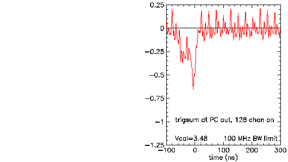
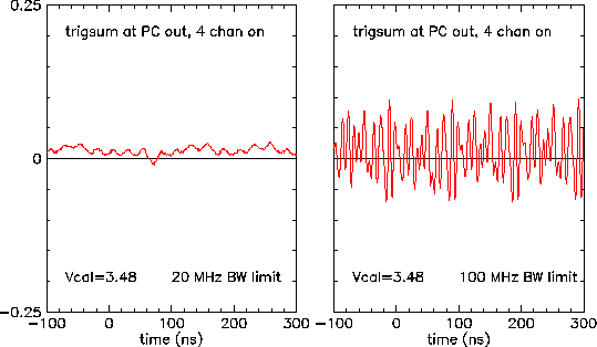
Check the waveform integrity of the 10MHz, 40MHz, and PECL clocks going into
the MCM. Here are examples of these clocks at the input connector
of the first MCM:
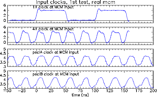
If the clocks do not look right, Make sure that there are terminating resistors at the 50-pin ZIF connector end of the clock lines which are driven by the buffers on the Power-Comm boards.
2. Download the Xilinx program, send the serial string
With the LabView program, download the program. As far as I can understand, pin 23 on the input connector (SD_OUT) will be +0V if the FPGA DONE line is set and +5V if it is not (i.e. it is "backwards"). This is the only way to check the DONE line on the real MCM's. This state is also indicated by the "DONE" light in the program. You should also see the analog current to the MCM change from about 0.5 to about 0.7 A when you download the MCM.
Follow this link for suggested intial settings of the serial string quantities. This is taken partially from experience and partially from a document written by N. Ericson etal You can set this set of serial string values by clicking on "start values" in the serial string menu.
The serial string should come out on the ser_data_out (p-23 of the MCM connector). However, you need to send the string twice to see the output -- it does not come out the first time. To look at this, set the scope on the 1 ms/div scale. You can use "repeat on" in the serial string section, which sends the serial string repeatedly. Trigger from pin-22 on the extender board (SER_DATA_IN). Touch the scope probe to TP2, 3, 4, in sequence to follow the data internally through the MCM. Finally look at pin 23 (the output). Check what comes back is the same as what goes in.
Use the "readback" button to readback the serial values loaded and make sure they are the same as what was sent. The "OK" light next to the readback button should come on.
If you used it, turn "repeat off" in the serial string section.
There is only one dac (VFB_RES on TGV1 = TP9)
which can be tested directly at a test point.
Only if there are problems with the serial readback or with the
serial data out line, check this DAC.
Try a few voltages, some results from the first evaluation lot
MCM are shown in the following table:
| DAC setting Volts | measured at TP9 Volts 5.020
| 4.77
| 4.781
| 4.77
| 4.622
| 4.60
| 4.304
| 4.25
| 3.508
| 3.47
| 3.030
| 2.95
| 2.473
| 2.34
| 1.996
| 1.84
| 1.518
| 1.32
| 0.961
| 0.80
| 0.484
| 0.28
| 0.324
| 0.12
| 0.165
| 0.06
| 0.086
| 0.06
| 0.006
| 0.06
| 5.02
| 4.77
| |
In the tests below on the ADC ramp, two other DACs (Iref and Vref on AMU/ADC 1) can be tested indirectly. Some of the heap manager serial string bits are also tested below.
3. Check data packet format
| Data word(s) correlated mode | Data word(s) raw mode | contents | expected range of hex values (not counting parity bit) 1
| 1
| Event counter (upper byte)
| 0 -- 3F
| 2
| 2
| Event counter (lower byte)
| 0 -- 3FF
| 3
| 3
| beam counter
| 0 -- FF
| 4
| 4
| AMU cell pre
| 0 -- 3F
| 5
| 5
| AMU cell post
| 0 -- 3F
| 6-261 (post-pre)
| 6-261 (pre data) | 262-517 (post data) Data
| 0 -- 3FF
| 262
| 518
| vertical parity
| 0 -- 3FF
| |
4. Inject charge using Cal-Enable mode and Bench Cal trigger
Here are some typical responses to difference Vcal values. Typically, individual chips seem to vary about 20% from these values.
| Vcal setting (volts) | typical ADC value
| 4.80
| 262 (hex)
| 4.30
| 1C1 (hex)
| 3.90
| 163 (hex)
| 3.48
| 104 (hex)
| |
5. Noise test
6. Spy channel test
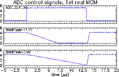
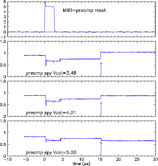
There are two sets of spy channels -- preamp spy channels (which look at preamp output) and AMU spy channels (which look at the AMU output). The preamp spy channels are controlled via "MUX1" in the serial string. The AMU spy channels are controlled via "MUX2" in the serial string. Both MUX outputs are controlled by AMU/ADC serial string bits. Set MUX1-OE=1 and MUX1-HIZ=1 for AMU/ADC1. Set MUX1-OE=0 and MUX1-HIZ=0 for all other AMU/ADCs. Set MUX2-OE=1 and MUX2-HIZ=1 for AMU/ADC1. Set MUX2-OE=0 and MUX2-HIZ=0 for all other AMU/ADCs. Set MUX1_0-4=00000 and MUX2_0-4=00000 (selects channel 0 from this AMU/ADC for output). Next, look at the TGV serial bits for TGV1. Set CAL_EN bit for first channel to 1 (bit 160) -- turning it "on". Set all other CAL_EN bits to 0 for TGV1. Set all CAL_EN bits to 0 for all other TGVs. Set VCAL for TGV1 to 3.48 Volts (=maximum pulse height). In heap manager serial string, set CAL_EN=1 and IREN=0. Next, click on "BENCH-CAL-ENABLE" followed by "Integrator Reset". Trigger the scope on mode bit 0 going into the MCM, in which case this signal occurs about 4 microsec after mode bit 0.
If you do this, you should see plots which look something like this (the arrow marks the charge injection):
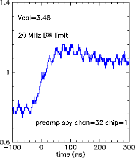
If you trigger on the spy channel itself and look at a finer timescale, you will see something like this:
For detailed descriptions of the output from mux1 (based on the PC/MCM, but more or less the same of the MCM) look here. Next, turn the charge injection for this channel off, (CAL_DIS=0 for bit 160). Make sure the signal (step) goes away. Next, turn the CAL_DIS bit back on (=1) and set VCAL=5.00. There should be no signal (5.00 corresponds to the minimum charge injected). Turn the MUX1 enable bits (MUX1-OE and MUX1-HIZ) off (=0) and make sure there is no signal. Turn MUX1 back on and select some other MUX address (e.g. 10000, which selects channel 2, counting from 1-32). Set VCAL=3.4 again, and make sure you do not see a signal (since you are now looking at channel 2 but injecting charge into channel 1). Test this with some other randomly selected channels in this AMU/ADC and in other AMU/ADCs.
Try a few channels in one preamp and at least one channel for every preamp. Also, try a few preamp disable bits, preferably one per chip. Do they turn off the spy channel output? Should should see a flat line, which will not be at ground potential.
Next, look at the AMU spy lines. These are controlled by MUX2-OE and MUX2-HIZ, which must both be set to one to turn a channel on. The address bits work like the preamp spy lines address bits. You should see traces like the ones below. The first level, marked with the arrows, it the significant voltage level. This is the voltage which is compared to the ramp. It should increase as Vcal is decreased. The voltage on the "flat" part of the AMU spy output is controlled by the Vcorr DAC. In this case it is at 1.3V.
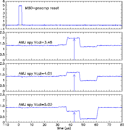
Try 2 or 3 Vcal values and a few MCM channels and make sure this
seems to work. Check at least one channel on each AMU/ADC chip.
Is it OK?
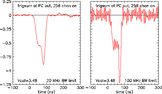
7. Check the Current-Sum discriminator
Here are some sample ISUM waveforms:
8. Temerature sensor
9. Final recommendation
Make a final recommendation -- should we accept or reject this MCM. Make any notes which seem important -- especially to explain why an MCM should be rejected.