|

|

|

|

After Miljko Bobrek made the most recent changes to the MVD's MCM Xilinx code, I studied the ADC response for two channels as the Level-1 delay was changed. This was all done with the internal charge injection which is controlled via the VCAL DAC on the TGV chip. This wirk was done with the Xilinx program called mcmc6.hex, which works with the correlator on in the AMU/ADC.
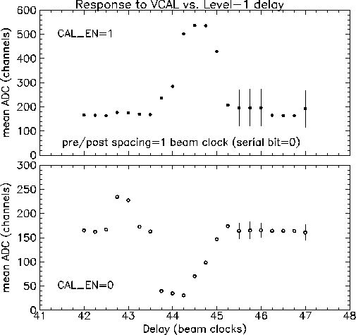
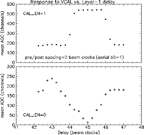
In each of the two following pairs of plots, the top plot shows the mean ADC value (based on 10 events) for a channel with the the calibration enabled -- i.e. charge is injected into the channel. The bottom plot in each pair shows the response for a channel which is disabled. The enabled channel responds as expected. The disabled channel shows a complicated response as the Level-1 delay is changed. Ideally, a disabled channel would show no response to changes in the level-1 delay. This seems to show that there is some interference between enabled and disabled channels.
The level-1 delay is controlled by 6 bits in the heap manager serial string. Four bits (bits 1-4) set the delay in units of beam clocks. This can be set from 32 to 47 beam clocks. The are two more "phase bits" (bits 7 and 8) which allow the level-1 delay to be adjusted in units of 1/4 of a beam clock. These phase bits seem to subtract from the number of beam clocks set with the other 4 bits. In the plots which follow, I have used the following table to translate the bit settings into a delay on the horizontal axis. For example, if the delay is set at 45 beam clocks, with phase bits 7, 8 = (1, 1), the point is plotted at a delay of 45 - 0.75 = 44.25 beam clocks.
| bit 7 setting | bit 8 setting | adjustment to level-1 delay
| 0
| 0
| 0.00 beam clocks
| 1
| 0
| -0.25 beam clocks
| 0
| 1
| -0.50 beam clocks
| 1
| 1
| -0.75 beam clocks
| |
The following plot shows the results when the pre/post spacing is 1 beam clock (serial string bit=0):

This plot is also available in ps format. The numbers shown on the plot are available here. In the plot above, the error bars represent the width (rms) of the distribution. From this plot, it seems that the best setting when using only 1 beam clock between the pre and post samples is "44.5" beam clocks delay, in other words, 45 beam clocks with the phase bits set to (1,0).

This plot is also available in ps format. The numbers on the plot are available here. No error bars are given on the plot above. From this plot, it seems that the best setting with the pre/post separation set at 2 beam clocks is 45 beam clocks with the phase bits both zero.