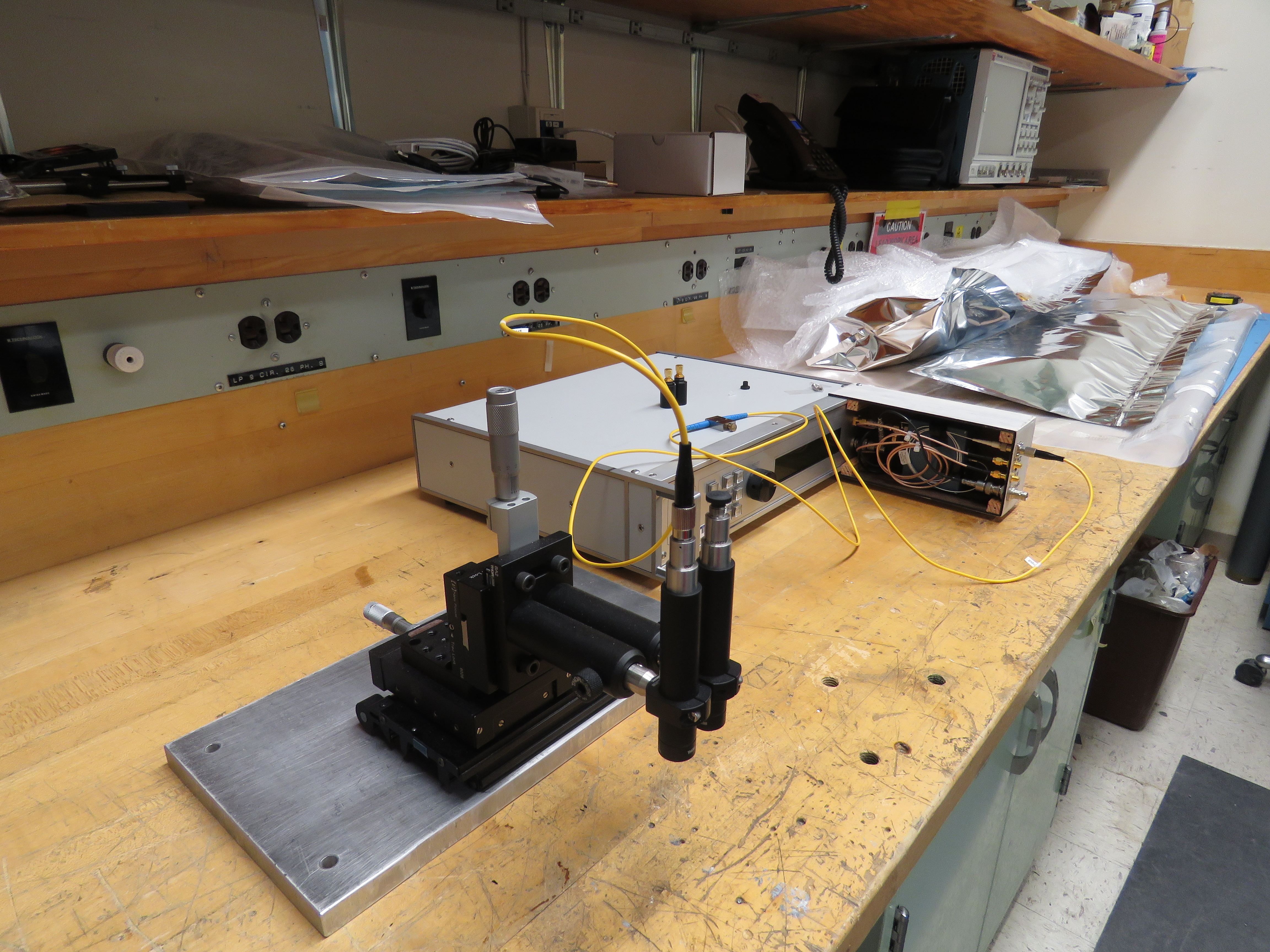
Our systemWe have two laser diodes we can choose between: QPhotonics QFLD-850-20SAX and QFLD-1064-10SAX. These are 850 nm/20 mW and 1064 nm/10 mW respectively, and have fiber pigtails built in. The laser diodes are driven by a fast pulse generator: AVTech AVO-9A-B-P, which has a max rep rate of 1 MHz and pulse width from 0.4-4 ns. For safety, we want the diode semi-permanently connected to the pulse generator: this is accomplished by enclosing the pulse generator output port and the diode in a box. This is meant to ensure that a user cannot easily connect the diode to another source.
|
|
SLAC system, for referenceOur system is largely a duplicate of a laser test stand that has been used at SLAC for characterizing silicon microstrips. The SLAC system has a large motorized stage instead of our small hand-driven one, but the other components (pulse generator, laser diodes, optics) are very similar.
|
|
Calculations of desired laser powerEpitaxial layer of ALPIDE is 25 um thick: this is the region where charge is collected. Mean energy loss for a MIP is 388 eV/um, so 9.7 keV. (Most probable energy loss is lower by a factor of ~2.) The number of electron-hole pairs you get is (energy deposit)/(ionization energy), ionization energy is 3.67 eV in silicon (PDG 34.7.1). This calculator gives transmission coefficients of 0.27832 for 850 nm and 0.96848 for 1056 nm. This doesn't account for reflection losses of ~1/3 The number of electron-hole pairs you get is just the number of photons that are absorbed. How much laser energy do we need to simulate a certain MIP energy deposition? The amount of energy we need per laser pulse is (hc/(wavelength)) * ((MIP energy deposit)/(ionization energy)) / (1-transmission). For 850 nm: (h*c/(850 nm)) * ((9.7e3 ev)/(3.67 ev)) / (1-0.27832) = 0.856e-15 J. At nominal power 20 mW and pulse width 4 ns, a pulse would be 80e-12 J. Need 1.1e5 attenuation, about 50 dB or OD 5.0. For 1064 nm: (h*c/(1064 nm)) * ((9.7e3 ev)/(3.67 ev)) / (1-0.96848) = 15.7e-15 J. At nominal power 10 mW and pulse width 4 ns, a pulse would be 40e-12 J. Need 2.5e3 attenuation, about 34 dB or OD 3.4. For normal operation let's run with an OD 4.0 filter in the 850 nm lens tube, and OD 3.0 in the 1064 nm lens tube. |
|
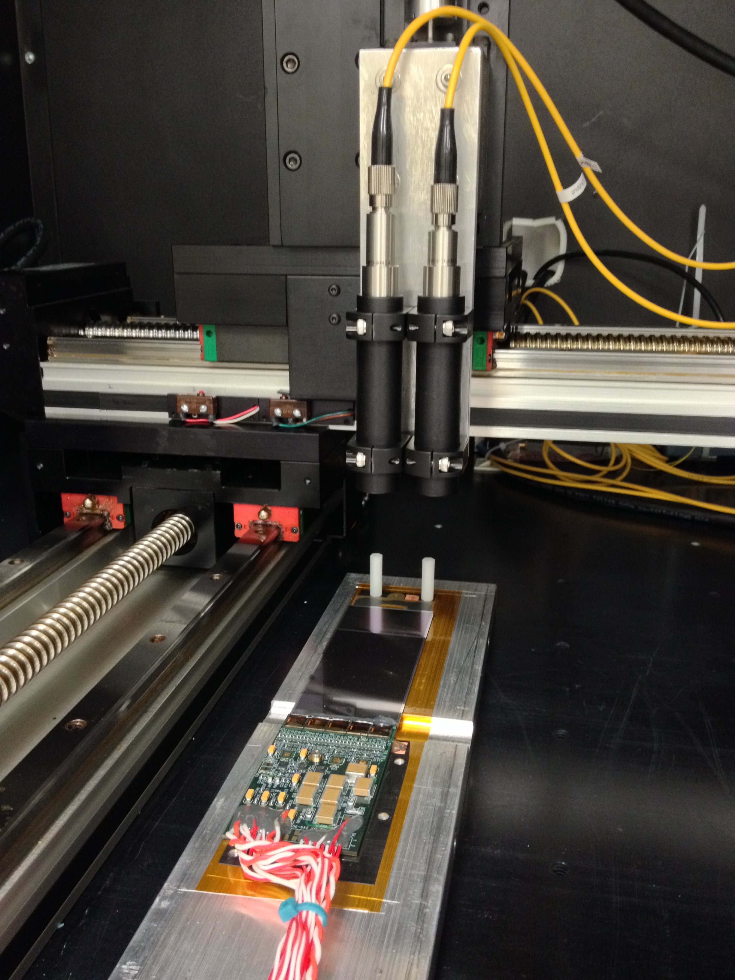
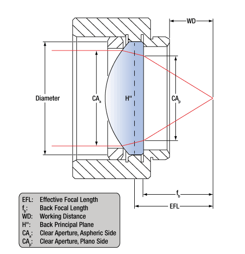
Laser focusThe beam diameter after the collimator is 2.4 mm for both collimators. The focal length is 25 mm for both lenses. The diffraction-limited spot size is 4*wavelength*focal length / (pi * beam diameter). This is the 1/e^2 diameter, and 86% of the power is inside this diameter. For 850 nm: 4*(850 nm)*(25 mm)/(pi * 2.4 mm) = 11.3 um. For 1064 nm: 4*(1064 nm)*(25 mm)/(pi * 2.4 mm) = 14.1 um. Both numbers are significantly smaller than the ALPIDE pixel dimensions: a circle with diameter 14.1 um fits very comfortably inside a square with sides 28 um. So we should be able to hit a single pixel. We could do math to see how much energy hits adjacent pixels. The lenses are not perfect, so there will be some broadening. Also, the beam only comes to a perfect focus at one Z, so the profile of the beam as it passes through the sensor is more like a cone. Not a big effect with a 50 um sensor. The 850 nm beam is mostly absorbed in the shallow part of the sensor, the 1064 nm beam illuminates the sensor uniformly. The "working distance" of our lenses is 19.6 mm: see figure to understand what this means. This is the required distance from the end of the lens housing to the ALPIDE. |
|
CalibrationWe have two photodiodes for calibration: one Si photodiode for 850 nm, and one InGaAs photodiode for 1064 nm. The Si photodiode is fast enough (1 ns rise and fall times) to resolve a short pulse. The InGaAs photodiode is slower (10 ns rise and fall) but it should still be possible to integrate to measure the pulse power. Si photodiode: about 0.35 A/W at 850 nm according to spec sheet, or 17.5 V/W into a 50-ohm load. A MIP pulse (0.856e-15 J from above) should make a voltage pulse of integral 1.5 e-14 V-s, which is too small to measure. But we can take out the OD 4.0 neutral-density filter, measure the 1.5 e-10 V-s pulse, and know that we have a MIP pulse when the filter is in. |
|
RF attenuatorsPrevious experience with AVTech pulsers is that the pulse shape is cleaner when you drive the max amplitude (13 V). So, run the pulser at max and use a fixed RF attenuator to bring the pulse height down to the nominal level for the diode. This also makes it impossible to destroy the diode by overdriving the pulser. For the 850 nm diode, nominal operating current is 45 mA, and nominal operating voltage is 1.9 V (max is 50 mA). So the nominal pulser voltage is (45 mA)*(50 ohm) + 1.9 V = 4.15 V. The necessary attenuation is 20*log10((4.15 V)/(13 V)) = 9.92 dB. Round up to be safe: we will attenuate by 10 dB for 850 nm. For the 1064 nm diode, nominal operating current is 50 mA, and nominal operating voltage is 1.33 V (max current is 55 mA). So the nominal pulser voltage is (50 mA)*(50 ohm) + 1.33 V = 3.83 V. The necessary attenuation is 20*log10((3.83 V)/(13 V)) = 10.61 dB. Round up to be safe: we will attenuate by 11 dB for 1064 nm. Jackie raised a concern about RF hazard, which is eliminated if we can limit the pulser output to 100 mA. We did this by installing a 6 dB attenuator inside the pulser chassis. So the attenuators on the diodes should be 4 dB and 5 dB. |
Sho Uemura Last modified: Thu Jan 24 12:08:32 MST 2019