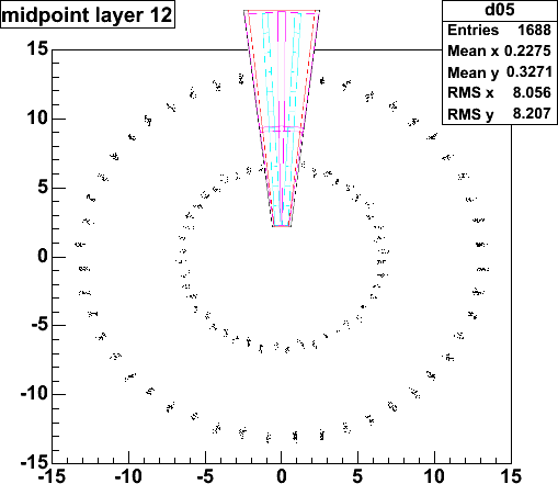
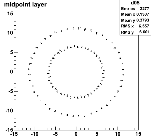
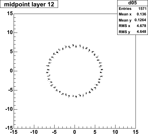
The following plots look at a single column of strips in the first
plane ('layer 9') of the cone DOE detector ('type 1'), using central
gold-gold events, with the event vertex at z=0.
This is the part of the detector where occupancies are the highest.
(files /phenix/data07/hubert/pythia2/
auau/ancsvx_auau_typeX.root,
where X is 1-4)
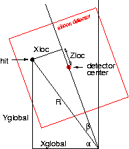
I look at the smallest readout unit, a single column of ministrips, serviced
by 5 readout chips (outlined in dark blue in the figure).
| 
|
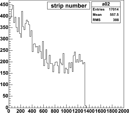
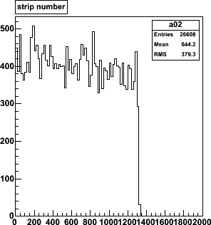
| This is the strip hit distribution for 9 AuAu events. The inner
silicon is 6.6 cm high, so that there are 1320 50-um strips. The hit
distribution is not flat, due to the non-uniform angular distribution of tracks
in the AuAu events.
| 
| 
|
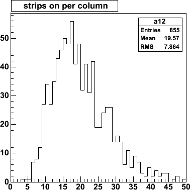
| Hits per column of strips for 9 events
(96 columns × 9 = 855 entries). 20/1320= 1.5% occupancy.
| 
| 
|
| Hits are clustered because of the track angles and the detector
tilt. Cluster sizes average 1.9, but there is a tail to large cluster
sizes, as shown in the inset (same plot, log scale). The cutoff at 20
is an artfact - my internal buffer size.
| 
| 
|
|
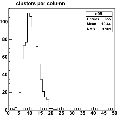
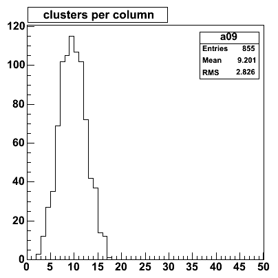
This is the distribution of clusters per column.
Typically there are 10 clusters distributed over 1320 strips, which
is a 0.76% cluster density (~= track density).
Typically there are 1000 tracks (10.44× 96) hitting the first cone
in a central AuAu event.
| 
| 
|
|
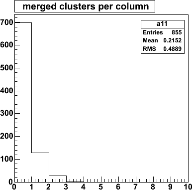
Number of overlapping clusters per column. Since the mean number of clusters
per 1320-strip column is 10, the mean distance between clusters is 132
strips. With the cluster size ~2, this means that most of these mergers
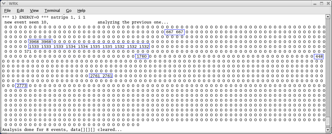
are not random overlaps. See this column
printout
| 
| 
|
|
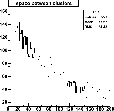
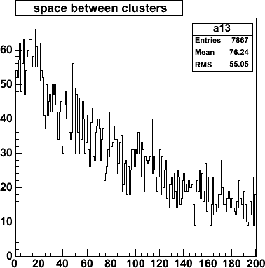
Distribution of empty space between clusters
| 
| 
|
|
Number of overlapping clusters per column. Since the mean number of clusters
per 1320-strip column is 10, the mean distance between clusters is 132
strips. With the cluster size ~2, this means that most of these mergers
are not random overlaps.
|
|
|
|
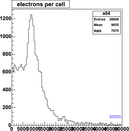
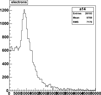
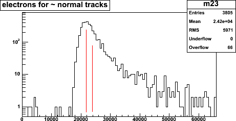
Electrons per hit
| 
| 
|