MCM Output Cable Quality Assurance Procedure
Toshiyuki Shiina
The University of Alabama in Huntsville
PHENIX-MVD-99-4, PHENIX Note 372
1. Introduction
2. Setup and Procedure
a) Continuity Test
b) Short Test
3. Result
Appendix A. MCM to Power Communication (or
Daughter) Board Pin Assignments
1. Introduction
This note documents the setup of the probe station and the procedure for
the electrical inspection of the 249 final production MCM output cables.
The electrical inspection is conducted after a brief (~ 5 min/cable) visual
inspection which searches for discontinuities. Only output cables
which pass the visual inspection should proceed to the electrical QA test.
2. Setup and Procedure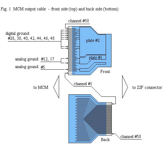
A handheld multimeter (FLUKE model #8020 B) was used to measure resistance
of traces. Continuity of a trace is assumed to be good when the resistance
reading is less than 0.5 Ohms, and insulation is
assumed to be good when the multimeter gives the overload reading ( > 20
MOhms.
a) Continuity Test
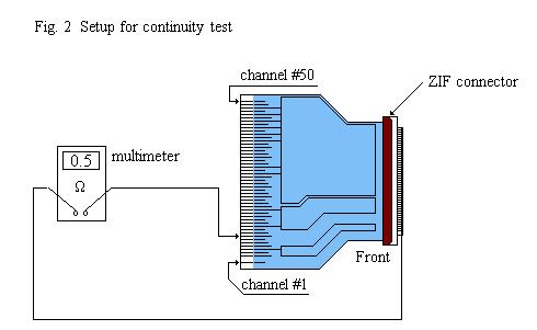
A ZIF connector (1ea Elco 50-contact, .5mm pitch
surface mount horizontal ZIF, 0.4 amp, model #
04-6240-050-003-800) was used to short one end of an MCM output
cable. (All the pins of the connector were soldered together. [Fig.
2] ) The shorted pins were connected to the negative pole of the
multimeter. And the positive pole was connected to a probe which
was used to make a contact to a trace of the output cable one by one to
complete the circuit for good continuity.
b) Short Test
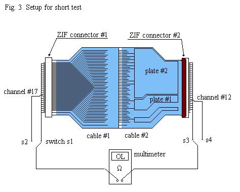
Two MCM output cables were tested for shorts at
one time. Cable #1 was connected to the connector #1 whose odd numbered
pins were shorted (except pin #17) and cable #2 was connected to the connector
#2 whose even numbered pins were shorted (except pin #12). The pin
#17 in the ZIF connector #1 was extended separately to avoid the short
circuit through the ground plate #2. The pin #12 was extended separately
in the ZIF connector #2 for the same reason. Two cables were pressed
against each other so that each trace of cable #1 made good contact to
the matching trace in cable #2. A set of two cables was tested for
shorts in three different configurations as follows.
Configuration 1: switch #1 - closed,
switch #3 - closed
The test voltage was applied
between the even numbered traces except #12 and the odd numbered traces
except #17.
Configuration 2: switch #2 - closed, switch
#3 - closed
The test voltage was applied between
the even numbered traces and the trace #17 .
Configuration 3: switch #1 - closed, switch
#4 - closed
The test voltage was applied between
the trace #12 and the odd numbered traces.
3. Result
All 249 production MCM output cables were thus tested
and numbered. No discontinuous trace was found among 12201 traces
(= 49 traces * 249 cables). Two cables were found to have shorts.
(cable #1 and #143)
They will not be used in the final assembly of MVD.
Appendix A. MCM to Power Communication (or Daughter)
Board Pin Assignments
MCM Output Cable Connector
(1ea Elco 50-contact, .5mm pitch surface mount horizontal ZIF, 0.4 amp,
model #
04-6240-050-003-800)
1. sil_bias (silicon detector bias)
2. (no connection, no trace)
3. sil_bias_return (silicon bias return)
4. +5V analog, tgv preamp
5. analog gnd, tgv, amu, isum amp
6. ((spare)) (grounded on power-comm board)
7. discr sum out
8. discr sum out gnd
9. +5V analog: comparator
10. analog gnd, comparator
11. +5Vanalog, amu, isum amp
12. analog gnd, tgv, amu, isum amp
13. - 5V analog, isum amp
14. +2.5V, Vmid
15. mcm temp sensor
16. preamp spy
17. analog gnd, tgv, amu, isum amp
18. amu spy
19. serial enable
;SEN
20. read back enable
;RBEN (enables mirror register read back)
21. serial clock
;SCLK (XCLK)
22. serial data in
;SDIN (XDIN)
23. serial data out
;SDOUT (xilinx done when PROG asserted)
24. serial latch
;SLATCH
25. xilinx program
;PROGB (clears FPGA program)
26. mcm_rst
;MCMRST (resets all data registers)
27. +5V, digital, HM & ADC
28. digital gnd, HM & ADC
29. +5V, digital, HM & ADC
30. digital gnd, HM & ADC
31. mode bit 0
32. mode bit 1
33. mode bit 2
34. mode bit 3
35. mode bit 4
36. mode bit 5
37. lvl-1 accept
38. digital gnd
39. mcm_DATA_OUT_clock
;4X Beam Clock
40. digital gnd
41. MCM_DATA_OUT_1
;serial data link #1
42. digital gnd
43. MCM_DATA_OUT_2
;serial data link #2
44. digital gnd
45. 9.5 MHz beam clock
46. digital gnd
47. 38 MHz clock
;4X Beam Clock
48. Digital Gnd
49. PECL clock A
;for ADC
50. PECL clock B
;for ADC
Note: 38 Mbit/sec MCM Data_Out and clock go to LVDS chips which are
mounted on the Power/Communication circuit board and Daughter board.