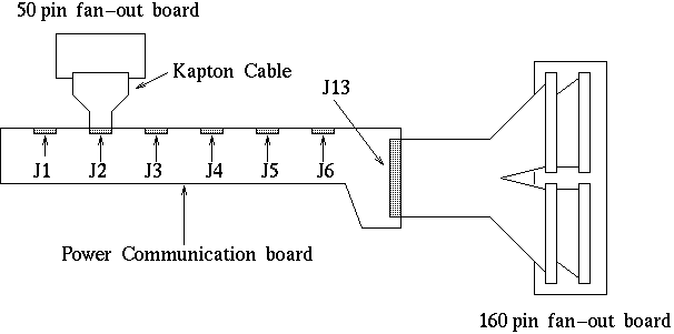
Fig 1. The arrangement of connectors on the right-side version power/comm board and two fan-out boards
YoungGook Kim, SangSu Ryu
Yonsei University, Korea
Sangkoo Hahn, Hubert van Hecke
Los Alamos National Laboratory
Aug, 1998
PHENIX-MVD-98-30, PHENIX Note 359
Contents
Introduction
The power communication boards of the MVD are mounted between motherboards and MCMs to enhance the integrity of signals over long distances from MCMs as well as to provide interconnection traces. Except for the temperature sensor and serial enable line, all interconnection lines are dedicated to the power and return. Besides these two major functions, some buffers have fan-out ability in order to distribute one signal from the motherboard over six MCMs.
We have tested the function of the pre-production power communication board(the right-side version). It had six 50 pin MCM connectors(J1 - J6) and a 160 pin mother board connector(J13). (For details of the connector types and pin assignments, see the signal document [1]). Unfortunately, it turned out that the even numbered pins and odd numbered pins on the 160 pin motherboard connector had been swapped. But for the test of the power communication board itself,this swapped pins did not make much difference because we had made an appropriate fan-out board for that 160 pin connector. At first, due to the cable length and impedance of the fan-out board, the input signals were distorted so that we could not observe any output signals. We lessened the distortion effect by putting terminators on the fan-out board.
This note will describe and summarize the results of two basic tests of the power communication board, the passive signal test and active signal test.
Fig 1. The arrangement of connectors on the right-side version power/comm board and two fan-out boards
Passive signal test
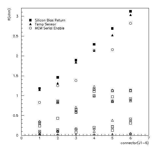
This test is to measure the pin-to-pin resistances of the signal lines for the direct connection between the 160 pin mother board connector and the 50 pin MCM connector. The signals that belong to this group go through only passive components, i.e resistor or capacitor. The resistances between two pins for each passive signal line were measured with a FLUKE 8060A multimeter across two fan-out boards. As for the mother board, the resistances of the two fan-out boards were subtracted from the total resistance to get the net resistance of each signal line. The subtracted values are shown in Table 1.
| Passive signal lines | Resistance[ohm](1) | |||||
|---|---|---|---|---|---|---|
| J1 | J2 | J3 | J4 | J5 | J6 | |
| Silicon detector bias | 10.29K | 10.18K | 10.24K | 10.18K | 10.23K | 10.26K |
| Silicon detector bias return | 1.18 | 1.46 | 1.89 | 2.29 | 2.69 | 3.12 |
| +5VA for TGV32 | 0.10 | 0.14 | 0.16 | 0.20 | 0.21 | 0.41 |
| +5VA return for TGV32 | 0.35 | 0.85 | 0.59 | 0.99 | 0.85 | 0.90 |
| +5VA return | 0.08 | 0.11 | 0.16 | 0.20 | 0.22 | 0.31 |
| +5VA for comparator | 0.30 | 0.83 | 0.63 | 1.16 | 1.14 | 1.14 |
| +5VA return for comparator | 0.24 | 0.43 | 0.65 | 1.16 | 1.12 | 1.12 |
| +5VA for AMUADC | 0.03 | 0.10 | 0.17 | 0.17 | 0.38 | 0.38 |
| +5VA return for AMUADC | 0.33 | 0.86 | 0.58 | 1.00 | 0.86 | 0.92 |
| -5VA | 0.08 | 0.12 | 0.71 | 1.23 | 0.87 | 0.87 |
| +2.5VA | 0.33 | 0.84 | 0.58 | 1.11 | 0.97 | 1.14 |
| Temp sensor | 1.15 | 1.31 | 1.84 | 2.13 | 2.52 | 3.03 |
| MCM serial enable | 0.83 | 1.25 | 1.38 | 2.14 | 2.16 | 2.82 |
| +5VD(related to J1-6,pin 27) | 0.02 | 0.00 | 0.00 | 0.00 | 0.10 | 0.03 |
| +5VD(related to J1-6,pin 29) | 0.00 | 0.00 | 0.08 | 0.00 | 0.13 | 0.03 |
| +5VD return(2) | 0.00 | 0.00 | 0.01 | 0.00 | 0.00 | 0.05 |
Except for the Silicon detector bias line which has a 10Kohm resistor between the MCM connector and the motherboard connector, each passive signal line had been expected to be shorted between the two connectors. The resistances of the Silicon detector bias line were measured as about 10K ohm and at large, the resistance values of the passive signal lines were below 1 ohm. Only three lines, Silicon bias return, temp sensor and MCM serial enable, showed relatively big resistance values between 1 and 3 ohm. (Only these lines are included in the legend of Fig 2.) Electronically, a group of signal lines which have the same function although each one of them belongs to a different 50 pin MCM connector, are shorted together onto a wide trace on the board so that there are no big differences in resistances between these signal lines. On the other hand, three signal lines with relatively big resistances have their independent traces separate from the other ones. This explains why the resistances of three lines, i.e Silicon bias return, temp sensor and MCM serial enable, were bigger than that of the other ones.
Active signal tests
The buffers residing on the power communication board are listed in Table 2.The description of the input signals which were used in the test, are also shown in Table 2.
| - | Input | Expected output | Note |
|---|---|---|---|
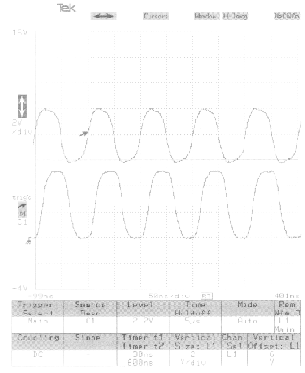
| Spy channel signal buffer | 1.0Vp-p, 100KHz | 1.0Vp-p +/-5%, 100KHz | op amp, gain -1 |
| PECL clock buffer | 4.0Vp-p, 40MHz | PECL logic level, 40MHz | fan-out buffer |
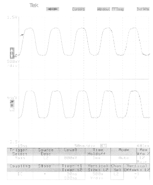
| LVDS drive buffer | 1.0Vp-p, 10MHz | 250mV +/-10%, 10MHz | - |
| Mode bit and Beam clock buffer | 4.0Vp-p, 10MHz | ACT logic level(0-5V), 10MHz | fan-out buffer |
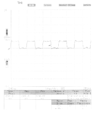
| Discriminator sum output buffer | 1.0Vp-p, 10MHz | 1.0Vp-p, 10MHz | op amp, gain 1 |
| Buffers for the serial data out, MCM program, read-back enable and MCM reset | 4.0Vp-p, 10MHz | ACT logic level(0-5V), 10MHz | - |
The test procedure is simple. First apply power for the power communication board. Three kinds of power, i.e +5V digital, +5V analog and -5V analog, are required to run all active components on the power communication board.
|
|
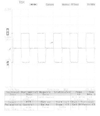
| a)Analog spy buffer output
(from J3 connector test) | b)PECL clock buffer output
(from J1 connector test) |
|
|
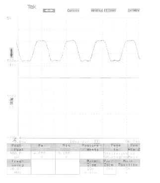
| c)LVDS driver buffer output
(from J5 connector test) | d)ACT logic buffer output
(from J2 connector test) |
|
|
| e)Discriminator sum buffer output (from J1 connector test) |
Fig 3. Output waveforms from different buffers
In Fig 3, five different output waveforms from the different kinds of buffers are shown. Each output accords well with the expected output. Here are the brief descriptions about the observed buffer outputs that appear in Fig 3.
All buffer outputs, which come out from either a six 50 pin MCM connector or a 160 pin mother board connector, were observed with a probe scope and verified as acceptable outputs.
Conclusion
The main goal of the above test was to verify the design of the pre-production power communication board as well as to confirm the normal operation of the board. Detected problems will be fixed in the next version of the power communication board.
At the beginning of the test, a minor schematic fault was detected. The odd pins and the even pins on the 160 pin motherboard connector (J13) were found to be swapped. This did not impact the tests of the power communication board itself.
The connectivity test, so called the passive test, has been done for all pass through signal lines. The measured resistance of Silicon bias line was about 10.2K. Besides this, the measured resistances ranged approximately from 0 to 3 ohm and consistently increased with the trace length. The other test, so called the active test to see if the buffers on the power communication board were working, have been implemented,too. We could not see any significant difference between the observed outputs and the expected outputs. Therefore, no problem was found on the above two basic function of the power communication board.
References