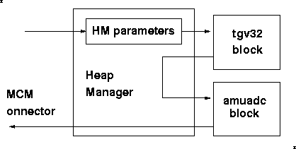
Figure 1. MCM Serial System Architecture
PHENIX-MVD-98-29, PHENIX Note 358
Introduction
A serial interface exists on each MVD MCM for multiple setup and control
operations. After a powerup condition the port is used to program the FPGAs.
Following this operation, the port switches automatically for control of the
multiple serial programming operations within the MCM. This document
addresses bothof the functions associated with the serial port - both FPGA
programming and slow serial operations.
MCM Serial System Architecture
A block diagram of the MCM serial string is shown in Figure 1. The string
passes through the Heap Manager where the HM parameters are stored, the tgv32
block (8 32-channel chips in series), back through the heap manager (feed
through only), through the AMUADC block (8 32-channel chips in series), and
through the heap manager (feed through only) and out of the MCM. The
multiple passes through the heap manager give some flexibility in dealing with
possible problems with serial string logic levels. Note that of the two FPGAs,
the serial string only passes through the controller FPGA.
| Bit # | Function |
|---|---|
| 1-9 | Not used. Load with any code you want |
| 9 | BTST |
| 10 | IREN |
| 11 | SLCT1 |
| 12 | SLCT0 |
| 13 | RAW_MODE |
| 14 | CAL_DIS |
| 15 | IR1 |
| 16 | IR0 |
| Bit # | Label | Function |
|---|---|---|
| 1-32 | CS_DIS[1..32] | Channel 1-32 Output Current Sum Disable |
| 33-96 | DIS_TWK[32..1] | Channel 32-1 a&b Discriminator Tweak |
| 97-128 | PRE_DIS[1..32] | Channel 1-32 Preamp Disable |
| 129-160 | CAL_DIS[32..1] | Channel 32-1 Calibration Disable |
| 161-166 | THRESH_DAC[5..0] | Discriminator Threshold DAC (MSB-LSB) |
| 167-172 | VMID_DAC[5..0] | Vmid DAC (MSB-LSB) |
| 173-178 | VGATE_DAC[5..0] | Vgate DAC (MSB-LSB |
| 179-184 | VFB_DAC[5..0] | Feedback Resistor Set Voltage DAC (MSB-LSB) |
| 185-190 | VCAL_DAC[5..0] | Calibration Voltage DAC (MSB-LSB) |
| Bit # | Label | Function |
|---|---|---|
| 1 | MUX2_OE | Mux 2 Output Enable |
| 2-6 | MUX2_0-4 | Mux 2 Address Bits 0-4 |
| 7 | CORR_SEL | Correlator Select control bit |
| 8-13 | DAC3_0-5 | DAC Vref Bits 0-5 |
| 14-19 | DAC2_0-5 | DAC Corr Bits 0-5 |
| 20-25 | DAC1_0-5 | DAC Iref Bits 0-5 |
| 26 | MUX2-HIZ | Mux 2 pull-down |
| 27 | MUX1-HIZ | Mux 1 pull-down |
| 28 | MUX1_OE | Mux 1 Output Enable |
| 29-33 | MUX1_0-4 | Mux 1 Address LSB |
| Bit # | Block Type |
| 1-16 | Heap Manager |
| 17-206 | TGV32 CHANNELS 256-225 |
| 207-396 | TGV32 CHANNELS 224-193 |
| 397-586 | TGV32 CHANNELS 192-161 |
| 587-776 | TGV32 CHANNELS 160-129 |
| 777-966 | TGV32 CHANNELS 128-97 |
| 967-1156 | TGV32 CHANNELS 96-65 |
| 1157-1346 | TGV32 CHANNELS 64-33 |
| 1347-1536 | TGV32 CHANNELS 32-1 |
| 1537-1569 | AMUADC CHANNELS 256-225 |
| 1570-1602 | AMUADC CHANNELS 224-193 |
| 1603-1635 | AMUADC CHANNELS 192-161 |
| 1636-1668 | AMUADC CHANNELS 160-129 |
| 1669-1701 | AMUADC CHANNELS 128-97 |
| 1702-1734 | AMUADC CHANNELS 96-65 |
| 1735-1767 | AMUADC CHANNELS 64-33 |
| 1768-1800 | AMUADC CHANNELS 32-1 |
| Input Code | IREF Out (Volts) | VMID Out (Volts) | VGATE OUT (Volts) | VFBRES OUT (Volts) | VCAL OUT (Volts) |
|---|---|---|---|---|---|
| 000000 (0) | 1.86 | 1.71 | 0.006 | 0.006 | 3.48 |
| 100000 (32) | 1.52 | 3.13 | 1.60 | 2.63 | 4.28 |
| 111111 (63) | 0.0 | 4.50 | 3.68 | 5.02 | 5.00 |
| DAC | Input Code (MSB ñ LSB) | Output Voltage |
|---|---|---|
| ITHRESH | 111111 | ~0 |
| VMID | 010000 | ~3.13 |
| VGATE | 000000 | ~0 |
| VFBRES | 111111 | ~5 |
| VCAL | 100000 | ~4.3 |
AMUADC Initial Serial Settings
Table 7 shows several input codes and associated output values measured for the AMUADC DACs. The DAC codes are in the following order: Bit 5 (MSB) - Bit 0 (LSB).
| VREF | VCORR | IREF | VREF Out (dc Volt) | VCORR Out (dc Volt) | IREF Out (dc uA) |
|---|---|---|---|---|---|
| 000000 | 000000 | 000000 | <0.4 | <0.15 | >70.0 |
| 000001 | 000001 | 000001 | 0.4 | 0.16 | 71.3 |
| 000010 | 000010 | 000010 | 0.48 | 0.20 | 70.2 |
| 000100 | 000100 | 000100 | 0.63 | 0.27 | 67.7 |
| 001000 | 001000 | 001000 | 0.93 | 0.42 | 63.0 |
| 010000 | 010000 | 010000 | 1.56 | 0.74 | 53.8 |
| 100000 | 100000 | 100000 | 2.73 | 1.30 | 35.9 |
| 111111 | 100000 | 100000 | 4.80 | 1.30 | 35.9 |
| 100000 | 111111 | 100000 | 2.73 | 2.50 | 35.9 |
| 100000 | 100000 | 111111 | 2.73 | 1.30 | <2.0 |
Approximate initial setpoint values for the AMUADC DACs are Vref DAC ~ 4.5 V,
Vcorr DAC ~ 1.6 V, and Iref DAC ~ 10mA. Table 8 provides the suggested initial
settings for each AMUADC ASIC serial string.
| Bit # | Label | Initial Settings For Testing | Function |
|---|---|---|---|
| 1 | MUX2_OE | 0 | Mux 2 Output Enable |
| 2-6 | MUX2_0-4 | 0 | Mux 2 Address Bits 0-4 |
| 7-12 | DAC3_0-5 | 111100 | DAC Vref Bits 0-5 |
| 13 | CORR_SEL | 1 | Correlator Select control bit |
| 14-19 | DAC2_0-5 | 101000 | DAC Corr Bits 0-5 |
| 20-25 | DAC1_0-5 | 110101 | DAC Iref Bits 0-5 |
| 26 | MUX2-HIZ | 0 | Mux 2 pull-down |
| 27 | MUX1-HIZ | 0 | Mux 1 pull-down |
| 28 | MUX1_OE | 0 | Mux 1 Output Enable |
| 29-33 | MUX1_0-4 | 0 | Mux 1 Address LSB |
The value of Iref depends strongly on the frequency of the digital clock. Check the ramp for eack frequency.
The chips will not work if the smoke inside gets out.