![[introduction]](../../../gifs/arrow.marble.left.gif)
|
![[LDO regulator test]](../../../gifs/arrow.marble.right.gif)
Up to the index
| Next page
| |
![[introduction]](../../../gifs/arrow.marble.left.gif)
|
![[LDO regulator test]](../../../gifs/arrow.marble.right.gif)
Up to the index
| Next page
| |
1. Necessary information for the test
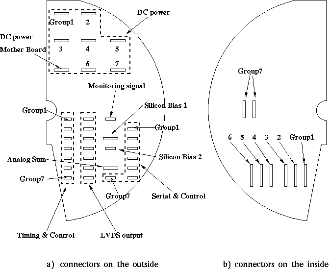
Before starting the test, we determined the function of each connector on the Mother Board. Fig1 shows the arrangement of connectors.

Fig 1. Connector arrangement on the Mother Board
There are 33 connectors on the outside of
the Mother Board arranged by
function. In the case of Timing & Control, LVDS
output, and Serial & Control connectors, the
group1 connector is the top one and the group7
connector is the bottom one in Fig1(a).
On the inside, connectors are arranged by group. Six 160 pin
connectors(groups 1-6) plug into power/comm boards and two 80 pin connectors
(group7) plug into a daughter board.
We made various fan out boards, a 160 pin, an 80 pin, a 50 pin, a 40 pin, a 36 pin, a 26 pin, and a 20 pin fan out board. Referring to the signal document [3], a label that describes the name of each pin was posted on each fan out board.
2. Simple setup for the connectivity test

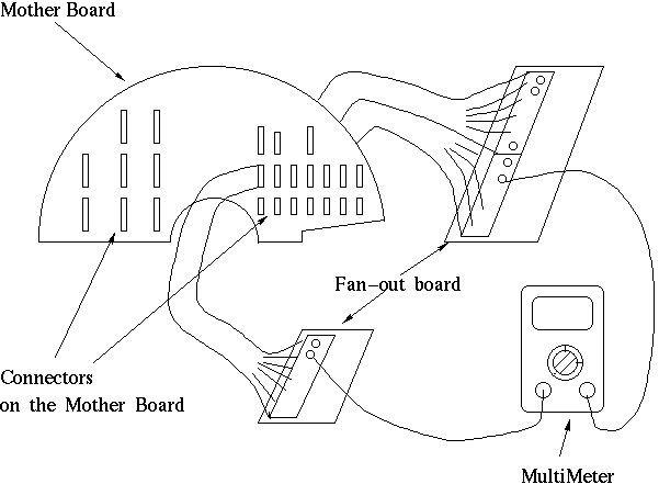
Fig 2. The resistance measurement using fan-out boards
We measured resistances for all pass-through signals. Starting with group 1, we identified a target signal then plugged the appropriate fanout board into the Mother Board. A pair of pins(or several pins in case of ground connection) with the same name were located,one pin on the inside and one pin on the outside of the board. Finally, a resistance value was measured with a FLUKE 8060A multimeter. This value included resistances of the two fan out boards, which we didn't want. Therefore we measured the resistance of each fan out board and subtracted it from the total measured resistance. The resistances of the fanout boards are shown below, in table 1. The resistance values appearing in table 2 of section 3 below exclude the portion from the two fanout boards.
| Fanout board | Resistance(ohm) |
|---|---|
| 160 pin | 0.38 |
| 80 pin | 0.38 |
| 50 pin | 0.39 |
| 40 pin | 0.35 |
| 36 pin | 0.37 |
| 26 pin | 0.35 |
| 20 pin | 0.35 |
3. Results
The resistance values, classified by the group # and signal function, are shown in table 2. Generally the measured values are distributed between 0.1 and 2.2 ohm, which we believe as acceptable. Comparing the values between groups, the measured resistances show the tendency to decrease when the group # increases from 1 to 6, which is due to the decrease of the trace length on the mother board. Because two 80 pin connectors for group 7 are far away from the 160 pin connectors, resistances for group 7 don't follow that trend. (See Figure 3.)
Because the analog discriminator sum is not used for groups 4-6,which relate to the outer layer strip detector, the table shows blank values for groups 4-6 analog sum signal connections. The below table doesn't contain the resistance values for ground connections. In fact, we had trouble with some DGND and AGND lines which are summarized at the end of this section. Except for these bad grounds, the remaining ground connections have relatively small resistance( < 0.2 ohm ) regardless of the group #.
| Group | Silicon Bias | LVDS | Serial & Control | Analog Sum | Timing & Control | |
|---|---|---|---|---|---|---|
| 1 | range | 1.45 ~ 1.78 | 0.94 ~ 1.33 | 1.08 ~ 2.16 | 1.19 ~ 1.30 | 0.67 ~ 0.89 |
| mean | 1.59 | 1.12 | 1.90 | 1.24 | 0.80 | |
| 2 | range | 1.35 ~ 1.70 | 0.85 ~ 1.16 | 1.57 ~ 1.96 | 1.10 ~ 1.18 | 0.70 ~ 0.84 |
| mean | 1.48 | 0.97 | 1.76 | 1.14 | 0.75 | |
| 3 | range | 1.43 ~ 1.62 | 0.76 ~ 1.12 | 1.35 ~ 1.89 | 0.76 ~ 1.08 | 0.34 ~ 1.15 |
| mean | 1.50 | 0.87 | 1.62 | 0.92 | 0.52 | |
| 4 | range | 1.34 ~ 2.14 | 0.48 ~ 0.80 | 1.13 ~ 1.50 | x | 0.26 ~ 0.61 |
| mean | 1.46 | 0.61 | 1.30 | x | 0.37 | |
| 5 | range | 1.03 ~ 1.79 | 0.37 ~ 0.65 | 1.03 ~ 1.36 | x | 0.13 ~ 0.51 |
| mean | 1.21 | 0.47 | 1.16 | x | 0.26 | |
| 6 | range | 1.09 ~ 1.55 | 0.27 ~ 0.63 | 0.77 ~ 1.02 | x | 0.01 ~ 0.19 |
| mean | 1.18 | 0.36 | 0.89 | x | 0.07 | |
| 7 | range | 0.40 ~ 0.47 | 0.75 ~ 1.24 | 0.79 ~ 1.13 | 0.89 ~ 1.04 | 1.33 ~ 1.63 |
| mean | 0.44 | 1.10 | 0.92 | 0.95 | 1.48 | |