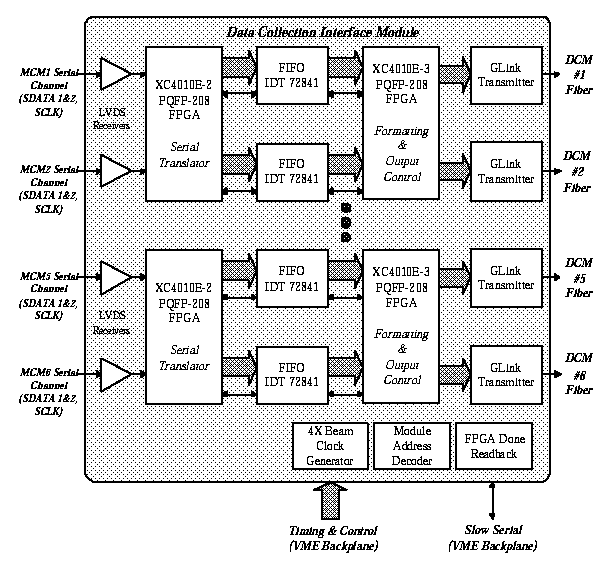
Figure 1. Data Collection Interface Module Block Diagram
M. N. Ericson, M. D. Allen
Oak Ridge National Laboratory, Oak Ridge, TN 37831-6006

Figure 1. Data Collection Interface Module Block Diagram
Each MCM serial stream consists of two data lines (SDATA1,2) coupled with a common clock line (SCLK). The system is functionally partitioned so that 2 MCM serial data channels are handled by a pair of Xilinx XC4010E FPGAs, allowing partitioning of the serial translator and data formatting functions. Table 1 details the contents of the serial string from the MCMs. Each 10-bit word sent contains a parity bit in the most significant bit.
| 10-Bit Word | Contents |
|---|---|
| 1 | event count (upper byte) |
| 2 | event count (lower byte) |
| 3 | beam count |
| 4 | AMU cell 1 |
| 5 | AMU cell 2 |
| 6-262 | ADC data (256 10-bit words) |
| 263 | checksum |
Table 1. MCM to DCIM Serial Data Packet Format
The start bit is defined as four rising edges of the SDATA1 line while SCLK is asserted high. The stop bit is four rising edges of the SDATA2 data line while the SCLK line is asserted high. When SCLK goes low, the requirement on the start and stop bit is reset, and the circuit begins again looking for consecutive edges on the data lines. When a start bit is detected, the data is clocked out and synchronized so that the rising edge of the SCLK is in the middle of each data bit. The first data word appears on SDATA1, and the second word is clocked out on SDATA2, beginning with the sixth bit of the first word on SDATA1. Thus, the serial data is staggered but is always synchronized with SCLK.
Serial data from the MCM is translated from LVDS to TTL levels, and is formed into parallel words by the Serial Translator FPGA, which checks parity for bit errors and logs framing errors before writing the data to a FIFO. From the data contained in the FIFOs, the Formatting and Output Control FPGA adds the module address (set by jumper on the DCIM PCB), header and trailer words, and 8 user words. Formatted event data packets, consisting of 20-bit words, are transmitted to the DCMs via GLink at ~19 Mb/sec (2X Beam Clock rate). The output data packet format for each of the GLink channels is outlined in Table 2.
| Sequence No. | 16-bit Word Format | CAV | DAV |
| 1 | all bits 'ON' | on | off |
| 2 | Detector ID | off | on |
| 3 | Event Number | off | on |
| 4 | Module Address | off | on |
| 5 | Flag Word | off | on |
| 6 | FEM Beam Clock Counter | off | on |
| 7 | AMU Cell Numbers | off | on |
| 8-264 | Data Block (257 Channels) | off | on |
| 265-272 | User Word Block (8 Words) | off | on |
| 273 | (Longitudinal Parity Word) | off | on |
| 274 | all bits 'OFF' | on | off |
Table 2. DCIM Output Data Packet Format
The DCIM is designed to handle serial data errors in limited fashion. Two error conditions are dealt with at the DCIM level -- framing and data errors. Framing errors include incorrect packet formatting, length, or start/end bit sequencing errors and are easily detectable. If a packet error occurs, a reserved bit in the 18-bit FIFO data is set and maintained for the first occurrence and every word thereafter for the duration of the packet. The errors and set bits are as follows:
|
1. underflow (not enough words before a stop bit) - bit 11
2. overflow (too many words before a stop bit) - bit 12 3. two consecutive start bits without a stop bit - bit 13 |
At initial installation of the PHENIX detector, the MCM to DCM ratio will be 2, changing to 1 as the remaining group of DCMs are purchased and installed at a future date. Operation in either mode (ratios of 2:1 and 1:1) is accomplished using the reprogrammability of the FPGAs and two channel enable bits ENDAT[0,1]. These bits indicate which of the 2 multiplexed channels (odd or even) transmit data over the shared GLink channel. The data formatting and control FPGA handles this function. Each channel is hard-wired on the PCB as either even or odd.
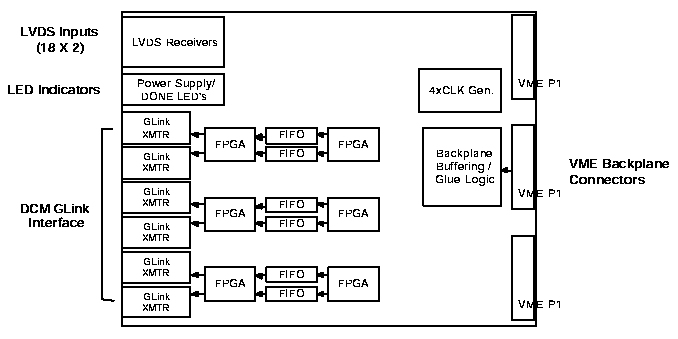
Three separate backplane connectors were selected for use in each crate -- one providing both power and signal distribution, and two additional connectors for supplying power. The estimated power requirements detailed in later sections provide the justification for this additional connector. The signals were grouped according to function, speed, and noise susceptibility, and assigned to the three connectors as shown in Tables 3, 4, and 5, which are found at the end of this document. Power was split into 4 separate supplies: +5V_D (digital power), +5V_GL (GLink power), and (12V_A (analog power). Grounds associated with each supply are also split accordingly to allow flexibility for crate grounding optimization. Additionally, extra signals (identified by * suffix) are assigned to each group and will be incorporated into module buffering for future expansion if necessary. Figure 2 shows the DCIM's I/O connectors and their general location on the PCB. Front panel mounted LED's were added to the design to allow external observation of the board power and FGPA DONE conditions.
Programming of the FPGAs is accomplished via the ARCNet-controlled VME backplane bus or a header on the board which is provided for testing purposes. The FPGAs are programmed as 3 groups of 2 serially connected units. Upon being programmed the DCIM has built-in capability for allowing polling of the 'DONE' bit of each FPGA individually using the backplane signals provided. This ensures proper system functionality. The FPGA's are clocked by a 4X Beam Clock signal which is produced on the board using a frequency synthesizer with the Beam Clock as its input. The frequency synthesizer is the exact design used in the Timing & Control Interface Module and other test fixtures associated with MVD.

Figure 2. DCIM Physical Layout and Connector Location
| Pin | Row A | Pin | Row B | Pin | Row C |
|---|---|---|---|---|---|
| 1 | --- | 33 | --- | 65 | --- |
| 2 | --- | 34 | GND_GL | 66 | --- |
| 3 | --- | 35 | --- | 67 | --- |
| 4 | --- | 36 | N/C | 68 | --- |
| 5 | --- | 37 | N/C | 69 | --- |
| 6 | --- | 38 | N/C | 70 | --- |
| 7 | --- | 39 | N/C | 71 | --- |
| 8 | --- | 40 | N/C | 72 | --- |
| 9 | GND_GL | 41 | N/C | 73 | GND_GL |
| 10 | --- | 42 | N/C | 74 | --- |
| 11 | GND_GL | 43 | N/C | 75 | --- |
| 12 | --- | 44 | --- | 76 | --- |
| 13 | --- | 45 | GND_GL | 77 | --- |
| 14 | GND_GL | 46 | --- | 78 | --- |
| 15 | GND_GL | 47 | --- | 79 | --- |
| 16 | --- | 48 | --- | 80 | --- |
| 17 | GND_GL | 49 | --- | 81 | --- |
| 18 | --- | 50 | GND_GL | 82 | --- |
| 19 | GND_GL | 51 | --- | 83 | --- |
| 20 | --- | 52 | GND_GL | 84 | --- |
| 21 | N/C | 53 | --- | 85 | --- |
| 22 | N/C | 54 | --- | 86 | --- |
| 23 | --- | 55 | GND_GL | 87 | --- |
| 24 | GND_GL | 56 | --- | 88 | --- |
| 25 | --- | 57 | --- | 89 | --- |
| 26 | --- | 58 | --- | 90 | --- |
| 27 | --- | 59 | --- | 91 | --- |
| 28 | --- | 60 | --- | 92 | --- |
| 29 | --- | 61 | --- | 93 | --- |
| 30 | --- | 62 | --- | 94 | --- |
| 31 | +5V_GL | 63 | +5V_GL | 95 | +5V_GL |
| 32 | +5V_GL | 64 | +5V_GL | 96 | +5V_GL |
Table 3. VME P1A Backplane Connector
(Module Flags and GLink Power(+5V_GL,GND_GL)
| Pin | Row A | Pin | Row B | Pin | Row C | ||||||||||||||||||||||||||||||||||||||||||||||||||||||||||||||||||||||||||||||||||||||||||||||||
|---|---|---|---|---|---|---|---|---|---|---|---|---|---|---|---|---|---|---|---|---|---|---|---|---|---|---|---|---|---|---|---|---|---|---|---|---|---|---|---|---|---|---|---|---|---|---|---|---|---|---|---|---|---|---|---|---|---|---|---|---|---|---|---|---|---|---|---|---|---|---|---|---|---|---|---|---|---|---|---|---|---|---|---|---|---|---|---|---|---|---|---|---|---|---|---|---|---|---|---|---|---|
| 1 | MODEBIT0 | 33 | --- | 65 | *CONF_TIM_X1 | ||||||||||||||||||||||||||||||||||||||||||||||||||||||||||||||||||||||||||||||||||||||||||||||||
| 2 | MODEBIT1 | 34 | GND_D | 66 | GND_D | ||||||||||||||||||||||||||||||||||||||||||||||||||||||||||||||||||||||||||||||||||||||||||||||||
| 3 | MODEBIT2 | 35 | --- | 67 | |||||||||||||||||||||||||||||||||||||||||||||||||||||||||||||||||||||||||||||||||||||||||||||||||
| 4 | MODEBIT3 | 36 | N/C | 68 | *CONF_TIM_X3 | ||||||||||||||||||||||||||||||||||||||||||||||||||||||||||||||||||||||||||||||||||||||||||||||||
| 5 | MODEBIT4 | 37 | N/C | 69 | *CONF_TCIM_X0 | ||||||||||||||||||||||||||||||||||||||||||||||||||||||||||||||||||||||||||||||||||||||||||||||||
| 6 | MODEBIT5 | 38 | N/C | 70 | *CONF_TCIM_X1 | ||||||||||||||||||||||||||||||||||||||||||||||||||||||||||||||||||||||||||||||||||||||||||||||||
| 7 | *MODEBIT6 | 39 | N/C | 71 | TCIM_GL_STAT | ||||||||||||||||||||||||||||||||||||||||||||||||||||||||||||||||||||||||||||||||||||||||||||||||
| 8 | *MODEBIT7 | 40 | N/C | 72 | TCIM_GL_RESET | ||||||||||||||||||||||||||||||||||||||||||||||||||||||||||||||||||||||||||||||||||||||||||||||||
| 9 | GND_D | 41 | N/C | 73 | GND_D | ||||||||||||||||||||||||||||||||||||||||||||||||||||||||||||||||||||||||||||||||||||||||||||||||
| 10 | BEAM_CLK | 42 | N/C | 74 | PA_SCLK_TIM | ||||||||||||||||||||||||||||||||||||||||||||||||||||||||||||||||||||||||||||||||||||||||||||||||
| 11 | GND_D | 43 | N/C | 75 | PA_SDIN_TIM | ||||||||||||||||||||||||||||||||||||||||||||||||||||||||||||||||||||||||||||||||||||||||||||||||
| 12 | ENDAT0 | 44 | --- | 76 | PA_SDOUT_TIM | ||||||||||||||||||||||||||||||||||||||||||||||||||||||||||||||||||||||||||||||||||||||||||||||||
| 13 | ENDAT1 | 45 | GND_D | 77 | PA_SEN_TIM | ||||||||||||||||||||||||||||||||||||||||||||||||||||||||||||||||||||||||||||||||||||||||||||||||
| 14 | --- | 46 | SCLK_DCM | 78 | --- | ||||||||||||||||||||||||||||||||||||||||||||||||||||||||||||||||||||||||||||||||||||||||||||||||
| 15 | GND_D | 47 | SDIN_DCM | 79 | GND_D | ||||||||||||||||||||||||||||||||||||||||||||||||||||||||||||||||||||||||||||||||||||||||||||||||
| 16 | LVL-1 | 48 | SCLK_TIM | 80 | GL_MUX2
| 17
| GND_D
| 49
| SDIN_TIM
| 81
| GL_MUX1
| 18
| DONE_RETURN
| 50
| GND_D
| 82
| GL_MUX0
| 19
| GND_D
| 51
| GL_STAT
| 83
| GND_D
| 20
| ---
| 52
| GND_D
| 84
| GL_SYNC
| 21
| N/C
| 53
| PROGB_DCM
| 85
| GND_D
| 22
| N/C
| 54
| GND_D
| 86
| MODADDR0
| 23
| ---
| 55
| GND_D
| 87
| MODADDR1
| 24
| GND_D
| 56
| PROGB_TIM
| 88
| MODADDR2
| 25
| PA_SCLK_TCIM
| 57
| GND_D
| 89
| MODADDR3
| 26
| PA_SDIN_TCIM
| 58
| *CONF_DCM_X0
| 90
| MODADDR4
| 27
| PA_SDOUT_TCIM
| 59
| *CONF_DCM_X1
| 91
| DONE_MUX0
| 28
| PA_SEN_TCIM
| 60
| *CONF_DCM_X2
| 92
| GND_D
| 29
| MRESET_TIM
| 61
| *CONF_DCM_X3
| 93
| DONE_MUX1
| 30
| MRESET_DCM
| 62
| *CONF_TIM_X0
| 94
| DONE_MUX2
| 31
| +5V_D
| 63
| +5V_D
| 95
| +5V_D
| 32
| +5V_D
| 64
| +5V_D
| 96
| +5V_D
| |
Table 4. VME P1 Backplane Connector
*CONF_DCM_X[0..3] Reserved for DCIM Configure Expansion
Small text indicates signal assignments not used by DCIM
| Pin | Row A | Pin | Row B | Pin | Row C |
|---|---|---|---|---|---|
| 1 | --- | 33 | --- | 65 | --- |
| 2 | --- | 34 | GND_A | 66 | GND_A |
| 3 | --- | 35 | --- | 67 | --- |
| 4 | --- | 36 | N/C | 68 | --- |
| 5 | --- | 37 | N/C | 69 | --- |
| 6 | --- | 38 | N/C | 70 | --- |
| 7 | --- | 39 | N/C | 71 | --- |
| 8 | --- | 40 | N/C | 72 | --- |
| 9 | GND_A | 41 | N/C | 73 | GND_A |
| 10 | --- | 42 | N/C | 74 | --- |
| 11 | GND_A | 43 | N/C | 75 | GND_A |
| 12 | --- | 44 | --- | 76 | --- |
| 13 | --- | 45 | GND_A | 77 | --- |
| 14 | GND_A | 46 | --- | 78 | --- |
| 15 | GND_A | 47 | --- | 79 | --- |
| 16 | --- | 48 | --- | 80 | --- |
| 17 | GND_A | 49 | --- | 81 | GND_A |
| 18 | --- | 50 | GND_A | 82 | --- |
| 19 | GND_A | 51 | --- | 83 | GND_A |
| 20 | --- | 52 | GND_A | 84 | --- |
| 21 | --- | 53 | --- | 85 | --- |
| 22 | --- | 54 | --- | 86 | --- |
| 23 | --- | 55 | GND_A | 87 | --- |
| 24 | GND_A | 56 | --- | 88 | --- |
| 25 | --- | 57 | --- | 89 | GND_A |
| 26 | --- | 58 | --- | 90 | --- |
| 27 | --- | 59 | --- | 91 | --- |
| 28 | --- | 60 | --- | 92 | --- |
| 29 | --- | 61 | --- | 93 | --- |
| 30 | --- | 62 | --- | 94 | --- |
| 31 | +12V_A | 63 | +12V_A | 95 | +12V_A |
| 32 | -12V_A | 64 | -12V_A | 96 | -12V_A |
Table 5. VME P1P Backplane Connector - Power Distribution Only