TGV32: A 32-CHANNEL PREAMPLIFIER CHIP FOR THE
MULTIPLICITY VERTEX DETECTOR AT PHENIX
C. L. Britton, Jr., M. N. Ericson, S. S. Frank, J. A. Moore,
M. L. Simpson, G. R. Young
Oak Ridge National Laboratory, Oak Ridge, TN 37831-6006
R. S. Smith
IBM, Research Triangle Park, NC 27709
L. G. Clonts
The University of Tennessee, Knoxville, TN 37996-2100
T. Parakkat
The University of Kentucky, Lexington, KY 40506
J. Boissevain, S. Hahn, J. S. Kapustinsky, J. Simon-Gillo, J. P. Sullivan, H. van Hecke
Los Alamos National Laboratory, Los Alamos, NM 87545
Review of Scientific Instruments, Vol. 70, No. 3, pp. 1684-1687, March 1999.
PHENIX-MVD-98-11, PHENIX Note 339
Abstract
The TGV32, a 32-channel preamplifier-multiplicity discriminator chip for the Multiplicity Vertex Detector (MVD) at PHENIX, is a unique silicon preamplifier in that it provides both an analog output for storage in an analog memory and a weighted summed-current output for conversion to a channel multiplicity count. The architecture and test results of the chip are presented. Details about the design of the preamplifier, discriminator, and programmable digital-analog converters (DACs) performance as well as the process variations are presented. The chip is fabricated in a 1.2-mm, n-well, CMOS process.
I. Introduction
The requirements of low-power consumption, fabrication utilizing a multi-chip module (MCM) process, a channel count of approximately 34,000, and flexible data handling make the Multiplicity Vertex Detector (MVD) of the PHENIX detector at RHIC one of the most challenging of the PHENIX detector subsystems. Additional requirements, which include a minimum 20:1 signal-to-noise ratio for a single Minimum Ionizing Particle (MIP) signal (which results in noise less than 2500 electrons rms) and discrimination of a 1/3 MIP event for the per-channel multiplicity discriminator, offer a yet greater set of problems.
This paper presents the architecture and the measurements of the 32-channel preamplifier known as the TGV32. The chip is fabricated in 1.2-
mm, nwell, CMOS and has a die size of 4.5 mm x 4.1 mm.II. Architecture
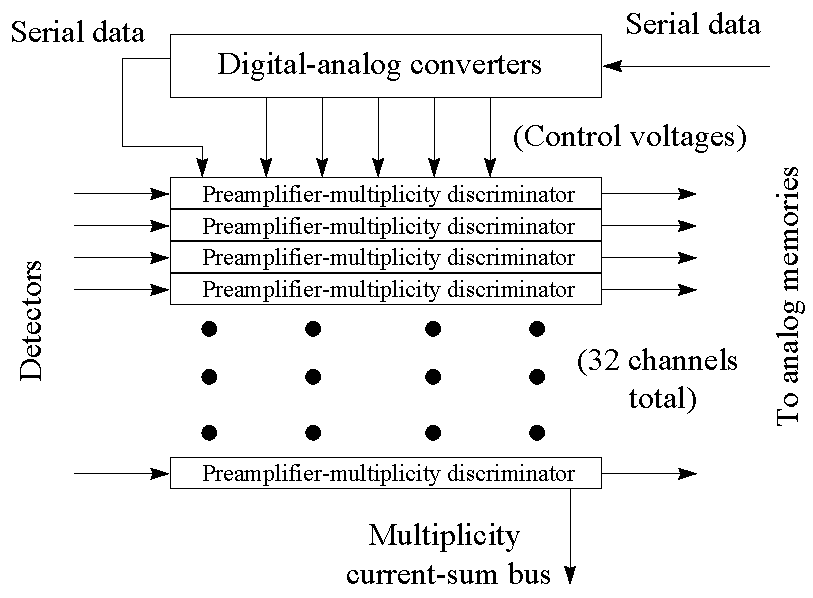
A block diagram of the full chip is shown in Fig 1. This includes five six-bit digital-analog converters (DACs) that control chip-wide functions such as preamplifier feedback resistor value, calibration voltage value, and discriminator threshold settings.

Figure 1. Chip block diagram.
A block diagram of two channels of the preamplifier is shown in Fig. 2. This includes the preamplifier, discriminator, current-sum output bus, and individual channel adjustments such as the calibration, noisy-channel disable, and discriminator offset adjustment. Each function of each channel is individually programmable through the use of a serial data string. A serial string 190 bits long is required to fully program the preamplifier chip. The entire serial string can be read back for verification without affecting the programmed values.
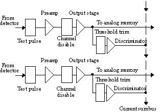
Figure 2. Two-channel block diagram.
III. Preamplifier
The preamplifier [1], whose block diagram is presented in Fig. 3, utilizes a PMOS cascode amplification stage for low 1/f noise. Signal-to-noise optimization is accomplished by varying the value of preamplifier feedback resistor because ac-coupled detectors with polysilicon bias resistors are being used in the MVD. The feedback resistor is a long-channel pmos device that is adjusted by another serially programmed DAC. The adjustable range of the resistor is from infinity to 500 ns.
The test pulse is accomplished by switching a capacitor between a voltage supplied by a DAC and the preamplifier +5 V supply. This difference allows each channel to be tested with a continuously variable analog voltage. The test pulse will enable outputs as great as 5 MIPs.
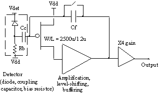
Figure 3. Preamplifier block diagram.
In this design, the feedback capacitor is split into two parts, Cf1 and Cf2, as shown in Fig. 4. Capacitor Cf1 is connected from the input to the dominant node. The other capacitor Cf2 is connected from the input to a source follower output. The second stage voltage amplifier also has two input capacitors, one from each node. Proper sizing of the four capacitors allows the gain and compensation of the linear chain to be adjusted almost independently.
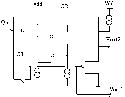
Figure 4. Preamplifier detail.
IV. Discriminator
The multiplicity discriminator [1, 2], whose block diagram is shown in Fig. 5, is used to determine the presence of an event above threshold on each channel. The current-mode outputs of 256 discriminators (eight chips) are summed to produce a multiplicity output whose amplitude is proportional to the number of fired discriminators. The design allows triggering at every beam crossing (105 ns) with no deadtime. The threshold for all 32 channels is set by a DAC-supplied voltage and the threshold range (the maximum and minimum values of the threshold) is set by another DAC. Because these two DACs control all 32 channels at once, channel-channel variations in input offset voltage are adjusted by a 2-bit fine adjustment which is serially programmed.
V. DACs
The basic DAC architecture [3] is shown in Fig. 6. A bias generator produces the bias voltages required by the DAC and all reference voltages and currents are derived using a single regulated voltage supply. The DAC circuit, composed of binary-weighted current sources, an offset current source, and a transimpedance output stage is shown in Figure 6. The resultant transfer function for the DAC is
![]() . (1)
. (1)
where n is an integer number bounded by 0 < n < 2m-1, for an m-bit DAC. The output range is configured by adjustment of Vmid, Ioffset, and the full-scale value of Ibinary. The current source values in the DAC are both proportional to 1/Rbias, resulting in an overall transfer function that compensates for the absolute resistance value changes of Rbias and Rf, resulting in DAC errors that are limited to the on-chip matching of resistance devices and MOSFETs [4, 5]. Temperature errors associated with the integrated resistors are also minimized since the temperature of on-chip resistors tracks well.
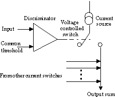
Figure 5. Discriminator block diagram.
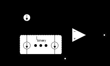
Figure 6. DAC Circuit Topology
VI. Programming
The serial string is programmed using four lines. Data is presented to the chip at the SDIN (serial data in) port. The data is clocked in on each positive-going edge of the SCLK (serial clock). After the data has been completely shifted in, the DCLK (data clock) line is pulsed and the data is loaded into each functions register. If a non-destructive readback of the data is desired for verification, the READBACK_EN (readback enable) line is held high for one cycle of the SCLK to load the shifting string and the data is then shifted out using SCLK. The chips are designed to be daisy chained so that only one set of lines is used to program 256 channels (eight chips). The output of each chip clocks the serial data out on the negative edge of the SCLK to ensure off-chip delays of the SCLK do not compromise the data and clock timing between chips. The data bit definitions are presented in Table 1.
Table 1. Bit definitions
|
Bit number (#1 is first in) |
Function |
|
1-32 |
Chan. 1-32 output current sum disable |
|
33-96 |
Chan. 32-1 A & B discriminator adjust |
|
97-128 |
Chan. 1-32 preamp. disable |
|
129-160 |
Chan. 32-1 calibration disable |
|
161-166 |
Discrim. Threshold (MSB-LSB) DAC |
|
167-172 |
Vmid (MSB-LSB) DAC |
|
173-178 |
Discriminator Vgate (MSB-LSB) DAC |
|
179-184 |
Feedback resistor voltage (MSB-LSB) DAC |
|
185-190 |
Calibration voltage (MSB-LSB) DAC |
VII. Results
A. Preamplifier
Some of the basic performance parameters are listed in Table 2. The charge gain vs. channel number is shown in Fig. 7. This was measured with approximately 15 pF input capacitance which was mostly due to wiring of the test board and charge terminator. The noise vs. channel number for a 13 pF input capacitance (wiring with no charge terminator) is presented in Fig. 8. This figure indicates some systematic increase in noise for increasing channel number but is not necessarily the same for other chips.
The channel-channel crosstalk was measured and found to consist almost entirely of coupling between wirebonds on the inputs. Without wirebonds present, the crosstalk was found to be less than 1 %. Testing with the actual detector cables will be performed at a later date to quantify the expected in-situ crosstalk.
Table 2. Basic performance parameters
|
Parameter |
Value |
|
Noise |
500 e + 72 e/pF |
|
Power dissipation |
1.7 mW/channel |
|
Risetime (0 pF) |
20 ns |
|
Risetime (13 pF) |
40 ns |
|
Minimum Threshold |
20 mV (1/4 MIP) |
|
Maximum threshold |
~ 400 mV (5 MIP) |
|
Maximum signal |
~ 1.5 V (19 MIP) |
The test pulse output vs. input code is presented in Fig. 9. The goal was to achieve greater than 4 MIPs full scale with approximately 0.25 MIP/input code step.
B. Discriminator
The discriminator outputs approximately 15
mA/channel when an event exceeds the threshold level. The current sum of eight preamplifier chips (256 channels) is fed into a CLC426 current-mode amplifier. The voltage output of the amplifier is then fed into a flash analog-digital converter. The output of a single channel is shown in Fig. 10. The top trace is the preamplifier output and the bottom is the output of the CLC 426. Only 32 channels are connected to the amplifier for this photo. The main feature of this pulse is that it is only a single beam crossing wide. This discriminator is active on every beam crossing.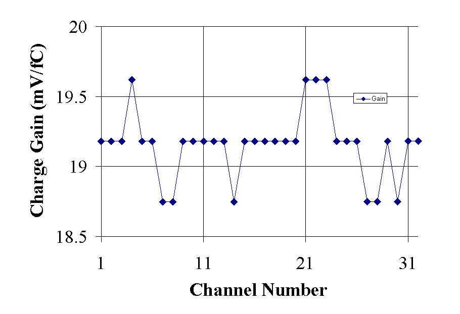
Figure 7. Charge gain vs. channel number.
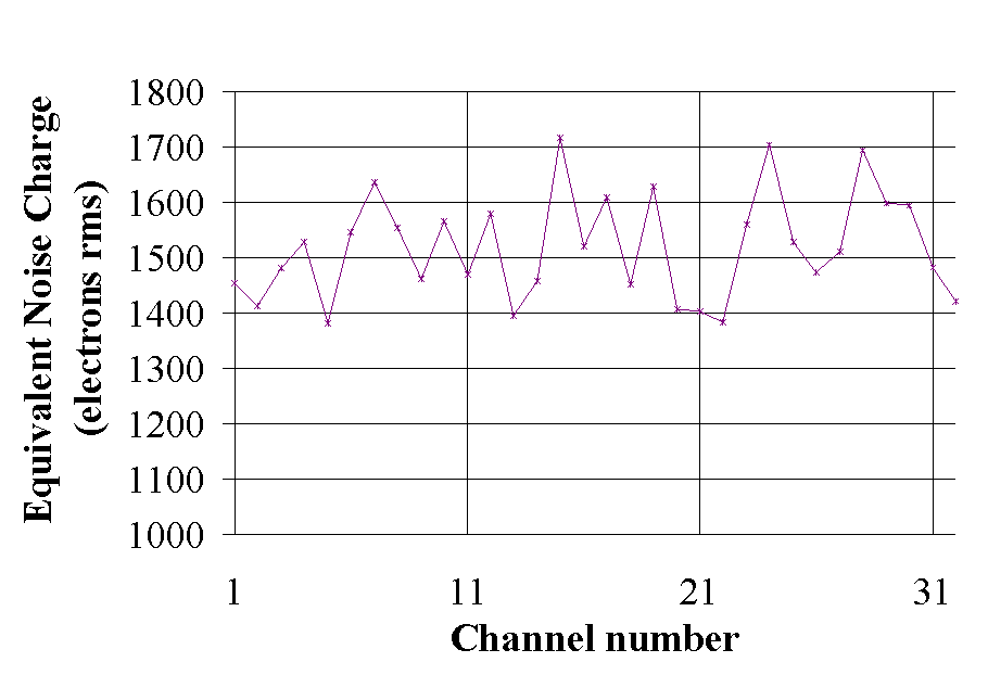
Figure 8. Noise vs. channel number with
13 pF input capacitance.
The discriminator was set up to have a nominal 30 mV threshold for an entire chip. The spread is plotted in Fig. 11 and indicates more deviation than we had anticipated. The heavy dotted line indicates the raw offset with no per-channel correction. The light dotted line indicates the data after correction using the two-bit correction. Channels 24 and 31 appear to be bad channels. We expected a variation of approximately ±10 mV but are seeing approximately two times that value.
The measurements were made with the discriminator just firing in the noise as shown in Fig. 12.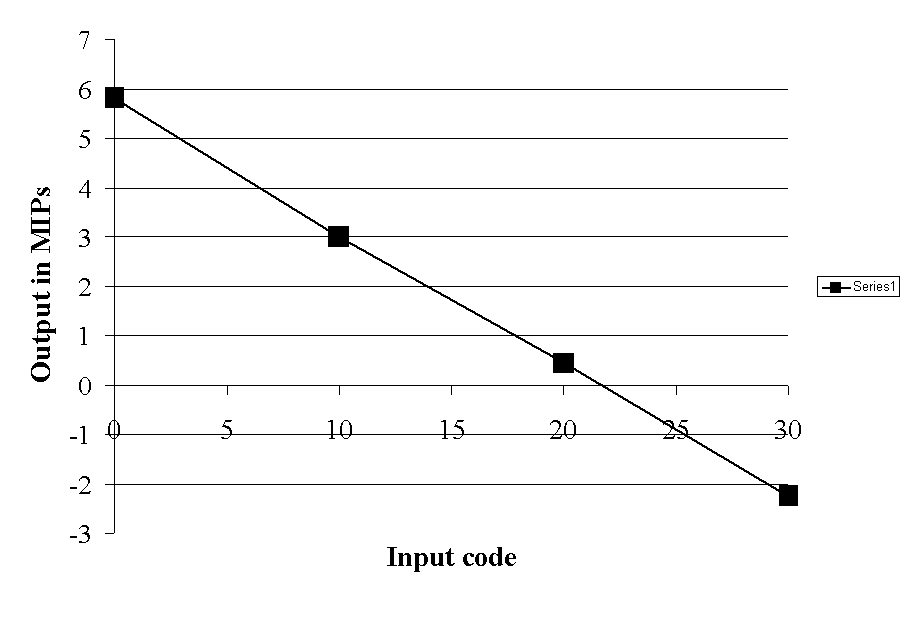 Figure 9. Test pulse vs. input code.
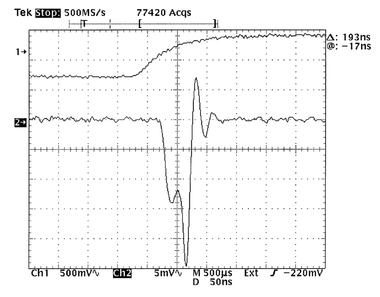
Figure 10. Output from preamplifier (top trace and discriminator (bottom trace).
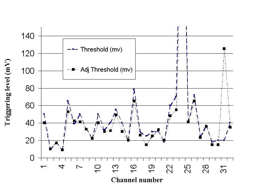 Figure 11. Discriminator sensitivities before and after adjustment.
The variations appear to be related to the process and possible slow preamplifier risetime due to the test fixture. The discriminator expects a preamplifier risetime of no greater than 60 ns. The test fixture design along with the calibrated charge terminator used for pulsing the chip gave a risetime of approximately 80 ns, longer than would be expected in actual practice. Some further testing will be performed on this aspect.

Figure 12. Preamplifier output (top trace) and discriminator (bottom trace) setup for threshold test.
For a set of simulated events in the PHENIX detector, the two dimensional plots of Fig. 13 show the multiplicity which would be detected with a perfect discriminator set at 0.25 mip (ideal multiplicity) vs. the mean multiplicity which would be detected using discriminators with the performance described in this paper (simulated multiplicity). The slope of the fitted line gives the average efficiency of the discriminators which is less than one because the threshold for most channels are above the ideal value of 1/4 MIP. Nevertheless, the linear relationship between the two means that a trigger based on these discriminators should work in this range of multiplicity values. The range of multiplicity values is goes up to the maximum values expected for Au+Au collisions at RHIC.
The top plot summarizes the discriminator's performance in a trigger based on the MVD strip detectors in the inner barrel. The average efficiency is about 74%. The relationship between the ideal and simulated multiplicities is not perfectly linear. The small departure from linear behavior seen at high multiplicities is a result of double hits in the strips. When the multiplicity is very high, some strips have more than one particle hitting them. The resulting signal is therefore larger and the discriminators appear to be more efficient.
 The bottom plot summarizes the discriminator's performance in a trigger based on the MVD pad detectors. The average efficiency is about 86%. This is higher than the efficiency seen for strip detectors due to the different geometry of the two types of detectors. The incident angle of most particles hitting the MVD pads is almost perpendicular to the surface. The observed signal is therefore the result of a particle passing through about 300 microns of Si -- this is our definition of a "1 MIP" signal. Most particles which hit the MVD strips enter the Si close to parallel to the surface of the Si. The strip pitch is 200 microns. The observed signal in the strips is therefore the result of a particle passing through 200 microns of Si (about 2/3 of a MIP). The apparent discriminator efficiency is therefore higher for pads than for strips. The relationship between the ideal and simulated multiplicities is closer to linear for the pads than for strips. This is because the probability of a two particles hitting a single pad is less than the double-hit probability for strips -- it is the double hits in the strips which causes the departure from linear behavior.
Figure 13. Efficiency of the multiplicity trigger for 64 channels of measured discriminator offsets.
VIII. Conclusions
We have presented measurements of the TGV32 preamplifier chip which will be used in the PHENIX MVD subsystem. The chip, a photograph of which is shown in Fig. 14, has 32 channels of preamplifiers and multiplicity discriminators an. Circuitry for linear pulse testing, feedback resistor control, and discriminator threshold adjustment in addition to channel disable is included on chip. The performance is as desired with the exception of the channel-channel threshold variation of the discriminators. This was found to be approximately twice the desired value. Simulations of the effect of the variations on the detector trigger efficiency show that the present performance should be acceptable however.
IX. Acknowledgement
The authors would like to thank Norma Hensley for her assistance in the preparation of the manuscript.
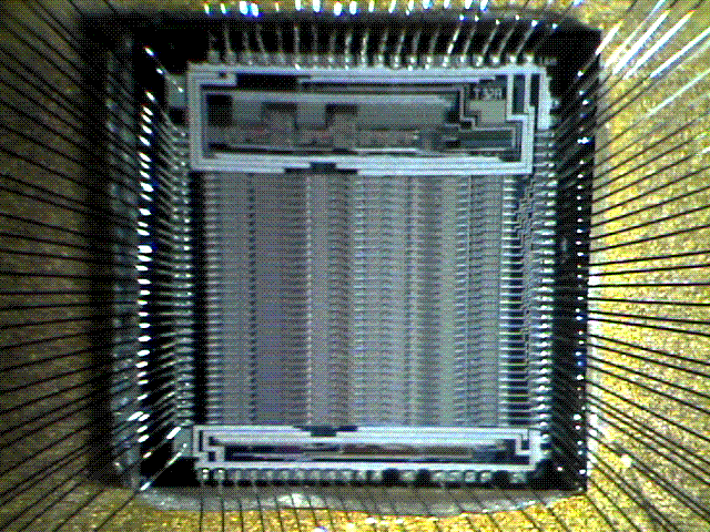
Figure 14. Die photograph.
X. References
[1] C. L. Britton, Jr., W. L. Bryan, M. S. Emery, M. N. Ericson, M. S. Musrock, M. L. Simpson, M. C. Smith, J. W. Walker, A. L. Wintenberg, G. R. Young, M. D. Allen, L. G. Clonts, R. L. Jones, E. J. Kennedy, R. S. Smith, J. Boissevain, B. V. Jacak, D. Jaffe, J. S. Kapustinsky, J. Simon-Gillo, J. P. Sullivan, H. Van Hecke, N. Xu, "Design and Performance of Beam Test Electronics for the PHENIX Multiplicity Vertex Detector", IEEE Trans. Nucl. Sci. Vol. 44, No. 3, June 1997 (283-288).
[2]
R. S. Smith, E. J. Kennedy, R. G. Jackson, M. L. Simpson, C. L. Britton, W. L. Bryan, U. Jagadish, G. R. Young, B. V. Jacak, J, Kapustinski, and A. Oscarson, "A Discriminator with a Current-Sum Multiplicity output for the PHENIX Multiplicity Vertex Detector", IEEE Trans. Nucl. Sci. Vol. 44, No. 3, June 1997 (389-392).[3]
M. N. Ericson, S. S. Frank, A. L. Wintenberg, J. S. Sam, C. L. Britton, Jr., and M. S. Emery, "A Configurable CMOS Voltage DAC for MultichannelDetector Systems", Presented at the 1997 IEEE Nuclear Science Symposium, Albuquerque, NM, Nov. 1997.[4] C. S. G. Conroy, W. A. Lane and M. A. Moran, "Statistical Design Techniques for D/A Converters," IEEE J. Solid-State Circuits, Vol. 24, No. 4, August, 1989.
[5] K. R. Lakshmikumar, R. A. Hadaway, and M. A. Copeland, "Characterization and Modeling of Mismatch in MOS Transistors for Precision Analog Design," IEEE J. Solid-State Circuits, Vol. SC-21, No. 6, December, 1986.