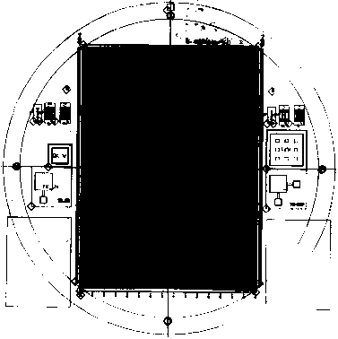
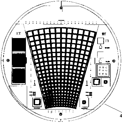
silicon strip and pad detectors
|
This shows a 256-channel silicon strip detector layed out on a 4" wafer,
surrounded by a number of small test structures.
The silicon is the standard 300 um thick. There are 256 200-um pitch strips (running vertically in this image). |
|
This shows a 12-column x 21-row silicon pad detector layed out on a 4" wafer,
surrounded by a number of small test structures.
Te smallest pads are about 2x2mm, and the biggest pads about 5x5mm. These detectors are made with a double-metal process. It allows readout traces to be deposited right over the pads, to bond pads along the top edge of the detector. Advantages of this technique are:
|