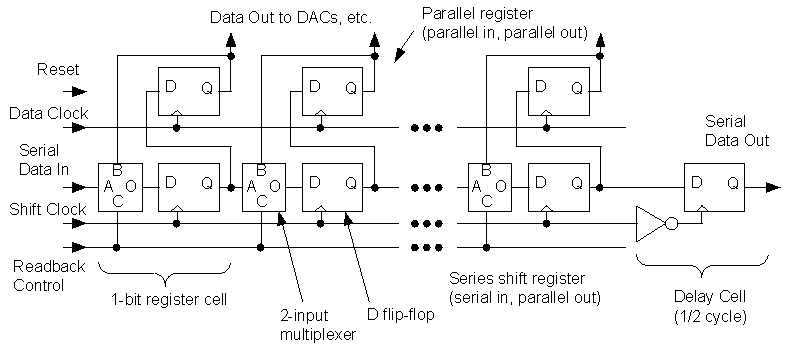
Figure 1. Architecture of serial data register.
Timing and Control Requirements for a 32-Channel AMU-ADC ASIC for the PHENIX Detector
1
M. S. Emery2, M. N. Ericson2, C. L. Britton, Jr.2, M.C. Smith2, S. S. Frank2, G.R.Young2, M. D. Allen3, L. G. Clonts3
2Oak Ridge National Laboratory, Oak Ridge, TN 37831
3
The University of Tennessee, Knoxville, TN 37996-2100
Abstract
A custom CMOS Application Specific Integrated Circuit (ASIC) has been developed consisting of an analog memory unit (AMU) and analog to digital converter (ADC), both of which have been designed for applications in the PHENIX experiment. This IC consists of 32 pipes of analog memory with 64 cells per pipe. Each pipe also has its own ADC channel. Timing and control signal requirements for optimum performance are discussed in this paper.
I. INTRODUCTION
The AMU-ADC was developed initially as two separate ICs with the intention of integrating the two pieces together. This merger was required due to space constraints of several of the PHENIX [1] subsystems, and the expected improvement to system performance. Detailed descriptions of the separate AMU and ADC circuits are found in references [2, 3].
Figure 1 shows a block diagram of the AMU-ADC. It consists of 32 parallel analog memory pipes, each pipe 64 cells deep. Each memory cell is a small capacitor, which stores the sampled input analog voltage, and read and write switches that connect the memory capacitor to either the Read amplifier or input signal, respectively. The output of each pipe is buffered through a Read amplifier to drive its corresponding ADC channel.

The Wilkinson topology ADC [4], which requires two analog references for its conversion process, VREF (reference voltage) and IREF (reference current). VREF sets the beginning voltage for the ramp waveform, and IREF controls the slew rate of the ramp. Both references may be supplied using on-chip programmable digital to analog converters (DACs). A third on-chip DAC provides the Correlator reference voltage [5].
True pipeline operation is enabled by the use of a buffer register located at the output of each ADC channel. This allows a new cell address to be read out to the ADC input and begin a new conversion at the same time that the previous result is being read out.
II. SERIAL DATA STRING
Several settings controlling operation of the AMU-ADC are set immediately following power up, but it is still desirable to allow programmable control of these settings. Therefore a serial data register is included to allow for the occasional reprogramming. These settings include a 6-bit word for each of the three DACs, control of the input and output spy multiplexers, and control of the Correlator circuit. Table 1 shows the name and function of each bit in the serial string, and is listed in order of first-in to last-in. An important feature of this serial register is the ability to read back the data to verify the contents of the latched serial data. Figure 2 shows the serial register architecture for loading and readout of the serial data. This architecture is consistent with that used for several other custom integrated circuits being developed at ORNL for PHENIX [6].
|
Bit # |
Label |
Function |
Bit # |
Label |
Function |
|
1 |
MUX2_OE |
Mux 2 Output Enable |
18 |
DAC2_4 |
DAC Corr Code bit 4 |
|
2 |
MUX2_0 |
Mux 2 Address LSB |
19 |
DAC2_5 |
DAC Corr Code bit 5 |
|
3 |
MUX2_1 |
Mux 2 Address bit 1 |
20 |
DAC1_0 |
DAC Iref Code bit 0 |
|
4 |
MUX2_2 |
Mux 2 Address bit 2 |
21 |
DAC1_1 |
DAC Iref Code bit 1 |
|
5 |
MUX2_3 |
Mux 2 Address bit 3 |
22 |
DAC1_2 |
DAC Iref Code bit 2 |
|
6 |
MUX2_4 |
Mux 2 Address bit 4 |
23 |
DAC1_3 |
DAC Iref Code bit 3 |
|
7 |
CORR_SEL |
Correlator Select control bit |
24 |
DAC1_4 |
DAC Iref Code bit 4 |
|
8 |
DAC3_0 |
DAC Vref Code bit 0 |
25 |
DAC1_5 |
DAC Iref Code bit 5 |
|
9 |
DAC3_1 |
DAC Vref Code bit 1 |
26 |
MUX2-HIZ |
Mux 2 pull-down |
|
10 |
DAC3_2 |
DAC Vref Code bit 2 |
27 |
MUX1-HIZ |
Mux 1 pull-down |
|
11 |
DAC3_3 |
DAC Vref Code bit 3 |
28 |
MUX1_OE |
Mux 1 Output Enable |
|
12 |
DAC3_4 |
DAC Vref Code bit 4 |
29 |
MUX1_0 |
Mux 1 Address LSB |
|
13 |
DAC3_5 |
DAC Vref Code bit 5 |
30 |
MUX1_1 |
Mux 1 Address bit 1 |
|
14 |
DAC2_0 |
DAC Corr Code bit 0 |
31 |
MUX1_2 |
Mux 1 Address bit 2 |
|
15 |
DAC2_1 |
DAC Corr Code bit 1 |
32 |
MUX1_3 |
Mux 1 Address bit 3 |
|
16 |
DAC2_2 |
DAC Corr Code bit 2 |
33 |
MUX1_4 |
Mux 1 Address bit 4 |
|
17 |
DAC2_3 |
DAC Corr Code bit 3 |
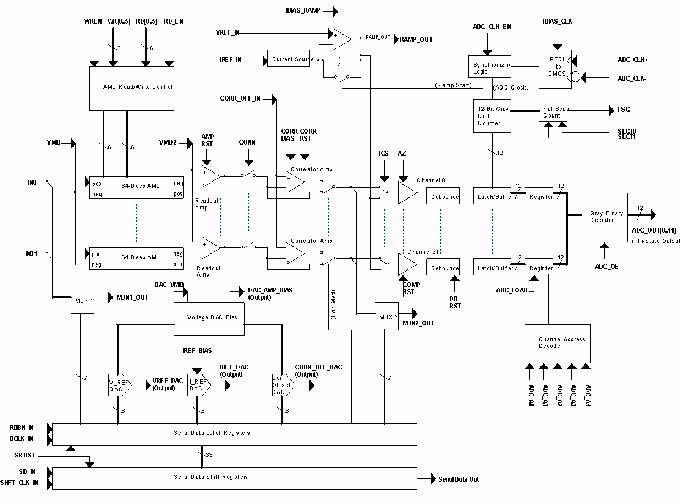
| Note the above picture is a reduced-size and quality gif file. Here
is the original gif file, but it is so big, that I kept it
separate (it crashes my X-terminal)
Here is a reduced-size ps file. Another way to get a good copy is to print out the entire document (see the top of the file) |
III. ADC OPERATION
The ADC section operates in either 12-, 11-, 10-, or 9-bit conversion modes. Although a user requiring lower precision could choose 12-bit conversions and simply truncate unnecessary bits, selecting a lower resolution significantly decreases the total conversion time. Equation (1) represents the time tconv needed by the ADC section to perform a conversion.

The variable n is the number of desired bits, f is the ADC clock frequency, and Toh is time needed for setup overhead. The variable n is the number of bits used in the conversion and would be either 9, 10, 11, or 12. The exponent is n- 1, instead of n, because the counter circuit counts on both the rising and falling clock edges and thereby reducing the time required by a factor of 2. This imposes a requirement for a 50% duty cycle clock to ensure equal bin width and good differential nonlinearity (DNL). The maximum measured clock frequency for the prototype chips has averaged 230 MHz.
The overhead time Toh includes several signals needed to initialize the ADC, but is actually dominated by the settling time needed for the AMU readout amplifier (discussed later).
Two ADC signals, Auto-Zero (AZ) and the Internal Comparator Switch (ICS), control CMOS switches used to pre-charge capacitors in the comparator circuits. The duration of the AZ and ICS signals must be sufficiently long to fully charge the capacitors due to the finite resistance of the switches and the resulting R-C time constant. Each of these require at least 100 ns for 12-bit accuracy.
The comparators are based on a dynamic switched capacitor design. A series input capacitor stores the input voltage across it, and then is compared with the ramp signal. When the ramp and input voltages are equal the comparator switches, causing the present value in the counter to be latched for that channel. The comparator output passes through a debounce circuit to improve noise rejection.
The AZ performs an autozero on the comparators to remove offset error voltages from the comparator block, resulting in much improved accuracy. During the time that AZ is high the comparators are in a linear region and draw about 0.7 mA per channel. Consequently AZ should not be asserted for an excessively long time in low power applications.
ICS controls whether the comparator input is connected to the input voltage (for storage on the input capacitor) or connected to the ramp signal. When ICS is a logical "0" the comparator input is connected to the AMU output. Conversely, when ICS is a logical "1" it is connected to the ramp output.
Conversion is initiated using the ADC_CLK_EN that enables the ADC clock signal used by the counter, and simultaneously starting the voltage ramp. Synchronizing circuitry ensures that the ramp generator and counter always start at the same time relative to the ADC clock. After the counter has reached full scale (either 9, 10, 11, or 12 bit) the Full Scale Count (FSC) flag is tripped which disables the counter and provides the indication of the end of conversion. If a channel fails to convert due to the input signal being either over-range or under-range, the full scale value remains in the ADC latch. Figure 3 shows suitable timing for the ADC operation. Note that the read enable signal denoted RD_EN in Figure 1 is called RENA in Figure 3.

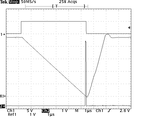
Optimum scaling of the ADC range is accomplished by adjusting the starting voltage level of the ramp and the ramp end point relative to the FSC. The full-scale voltage corresponds to VREF , provided by the VREF DAC. The ramp slews negative towards the ground voltage rail, its ultimate limit. The last 100 mV of the linear ramp will start to show some distortion, so for best linearity the slew rate should be adjusted by IREF such that FSC occurs when the ramp voltage is 100 mV or higher. If the user desires the minimum scale voltage to be something other than near zero volts, then the ramp slew rate may be adjusted such that FSC occurs at a higher voltage. Figure 4 shows a typical adjustment of the ramp relative to the FSC.
IV. AMU OPERATION
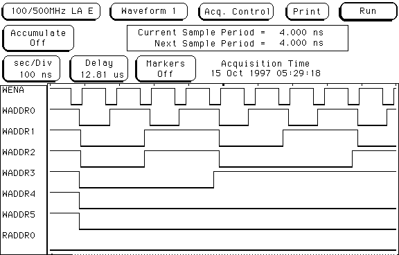
The analog memory section can be thought of as an analog equivalent of the digital random access memory (RAM). It stores a voltage at a specified cell address, and then later it can read out the specified cell address. Writing to the cell is performed by sampling an input analog voltage and storing it across a capacitor. The sampling rate will be the PHENIX beam clock frequency of approximately 9.4 MHz. The maximum writing rate is approximately 12 MHz due to tradeoffs in capacitor and switch size versus circuit layout area. Due to the time constant resulting from the resistance of the CMOS switches in the WRITE circuit and the memory cell storage capacitor, 40 ns is required to charge the memory storage capacitor to 12-bit accuracy. Figure 5 shows the timing diagram for writing to the AMU, with a Write Enable pulse duration of 50 ns. The write address bus (designated WADDR0 - WADDR5 in the timing figures) must be settled before WREN goes high. The write enable signal is denoted by WREN in Figure 1 and is called WENA in Figure 5.
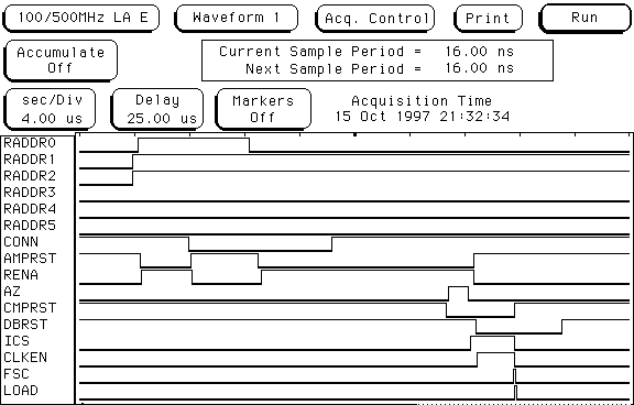
As previously mentioned, reading the AMU memory dominates the amount of time in the Toh term of Equation (1). Each AMU pipe has its own readout amplifier. When a read operation is not being performed the amplifier is maintained in a "reset" condition. This places the amplifier in a unity-gain buffer configuration with the input connected to the VMID2 voltage reference, which prevents both the input terminal of the amplifier from floating and the amplifier from saturating. Then the desired cell address is issued to the Read Address bus (designated RADDR0 - RADDR5 in the timing figures), followed by releasing the AMP_RST, finally followed by the read enable signal RD_EN. When this occurs the amplifier output will step from the VMID2 voltage level to that of the memory cell that is being read. The response of the amplifier depends upon the bias current, which is set using either an on-chip bias resistor or an external bias network connected to the CORR_BIAS pin. The amplifier response will be slew-rate limited when using the internal bias, but will settle to its final value in about 2.5 m s even for large steps. Increasing the bias current eliminates the slew-rate limitation, but the response is still limited by amplifier bandwidth. Again, the settling time needed is about 2.5 m s. Figure 3 shows the readout sequence.
The AMU also includes a correlator circuit which is used to look at the voltage difference between two different cell addresses in a pipe. The Multiplicity Vertex Detector subsystem [7] requires this mode of operation due to limited bandwidth available for data transmission. This voltage difference is obtained by a difference amplifier implemented with switched capacitors. The difference voltage is then presented to the ADC section for digitization.
The correlator amplifier is identical to the read amplifier, and is enabled by setting the CORR_SEL bit high in the serial data string. Figure 6 shows operation using the correlator. Note that the CONN signal remains constant under normal operation, but is pulsed when using the correlator to connect and disconnect the difference amplifier at appropriate times. Conversion time when in correlator mode is greatly increased since there are two AMU read operations. Actually, a total of four amplifier settling times must be allowed in this mode. The first cell read is stored in the correlator circuit while CONN signal is high and the switch is closed. Then the CONN switch is opened and the read amp is reset. Next, the second cell is read out. The read amplifier must be allowed to settle for each of the two read operations, plus settling for the reset. Then, the CONN switch is again closed, connecting the second cell’s value to the correlator circuit which gives the difference voltage between the two cells. Because this will be yet another voltage step, settling time must be provided again. A minimum of 10 m s (Toh in Equation (1)) is required before the actual ADC conversion can begin.
V. COMBINED AMU-ADC PIPELINE OPERATION
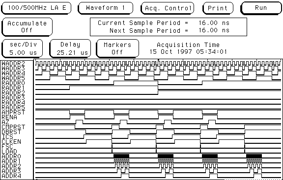
As mentioned earlier, an output data register is provided to store the results of the ADC conversion. This allows a previous conversion to be read out while a new conversion is taking place. The data readout process must be complete prior to the next LOAD signal. Figure 7 shows pipeline operation by performing four conversion cycles in less than 40 microseconds. In this test the ADC was operating in 11-bit mode and an ADC clock frequency of 200 MHz. The ADC channel address bus is designated ADDR0 - ADDR4 in the timing figures.
Reading out the digital data can be done at reasonably high rates. The actual limit will depend on the data bus loading characteristics, specifically the total load capacitance that the output drivers have to drive. Twenty Megahertz readout rates can be achieved with careful bus design.
VI. OPERATION IN THE PHENIX ENVIRONMENT
In the PHENIX environment, control of the AMU-ADC will be done by the Heap Manager [8, 9]. This includes a section referred to as the Address List Manager (ALM) [10]. As noted earlier the analog memory writing rate will be 9.4 MHz, corresponding to a period of 106 ns. Since a complete conversion cycle takes a minimum of about 10 m s, it is possible that a cell containing a signal of interest would not be digitized before the next AMU write cycle comes along and overwrites the data. The ALM functions to keep up with which cell addresses are of interest and remove these from the list of addresses available for writing fresh data. This function is quite complex since after a few conversion cycles the writing order can become considerably scrambled.
The AMU-ADC control signals are supplied by the Heap Manager. It includes a state machine which generates the appropriately timed signals using feedback from the FSC signal. When the FSC occurs (or after a sufficient amount of time without FSC occurring) the state machine drops the ADC_CLK_EN, issues the LOAD signal, and begins scanning out the digital data from the desired channels. The Heap Manager also formats the data into a defined packet for transmission to the next level of data collection.
VII. CONCLUSION
The AMU-ADC custom integrated circuit can be used in several different operating modes that allow the user to optimize throughput speed and the precision of the data to meet the requirements of varying applications. However, this flexibility makes the chip rather complicated to control correctly. Proper setup and timing of the various control signals required by this AMU-ADC integrated circuit have been presented. Differences between the normal non-correlator operating mode and operation with the correlator have been discussed. Pipeline operation of the device at high conversion rates has been demonstrated. The underlying reasons for the duration of the most important control signals have been discussed.
VIII. REFERENCES
[1] W.L. Kehoe, et al., PHENIX Conceptual Design Report, New York: Brookhaven National Laboratory, 1993.
[2] C.L. Britton, Jr., et al., "Design and Performance of Beam Test Electronics for the PHENIX Multiplicity Vertex Detector", IEEE Trans. Nucl. Sci., Vol. 44, No. 3, pp. 283-288, June 1997.
[3] M. S. Emery, et al., "A Multi-Channel ADC for Use in the PHENIX Detector", IEEE Trans. Nucl. Sci., Vol. 44, No. 3, pp. 374-378, June 1997.
[4] O. B. Milgrome, et al., "A 12 Bit Analog to Digital Converter for VLSI Applications in Nuclear Science," IEEE Trans. Nucl. Sci., Vol. 39, No. 4, pp. 771-775, 1992.
[5] M. N. Ericson, et al., "A Configurable CMOS Voltage DAC for Multichannel Detector Systems," submitted to the Proceedings of the 1997 IEEE Nuclear Science Symposium, Albuquerque, NM, Nov. 11-13, 1997.
[6] C. L. Britton, Jr., et al., "TGV32: A 32-Channel Preamplifier Chip for the Multiplicity Vertex Detector at PHENIX," submitted to the Proceedings of the 1997 IEEE Nuclear Science Symposium, Albuquerque, NM, Nov. 11-13, 1997.
[7] J. S. Kapustinsky, et al., "A Multiplicity Vertex Detector for the PHENIX Experiment at RHIC," submitted to Proceedings of the 4th International Conference on Position Sensitive Detectors, Manchester, UK, Sept. 9-13, 1996.
[8] M. D. Allen, "Development of an FPGA-Based Heap Manager for the PHENIX Multiplicity Vertex Detector," Master of Science Thesis, University of Tennessee, Knoxville, 1996, pp. 104-106.
[9] M. N. Ericson, et al., "Development of a Front End Controller/Heap Manager for PHENIX," IEEE Trans. Nucl. Sci., Vol. 44, No. 3, pp. 312-317, June 1997.
[10] M. N. Ericson, et al., "A Flexible Analog Memory Address List Manager for PHENIX," IEEE Trans. Nucl. Sci., Vol. 44, No. 3, pp. 1629-1633, June 1996.