MVD Cables Design Requirements

J. Boissevain, B. Jacak, J. Kapustinsky

November 19, 1995


This note gives some design requirements for the MVD, as requested by V. Borshchev from Kharkov. The information will allow further progress on the design of the microcables for the MVD, but is also of more general interest. Figure 1 shows a side view of the MVD, with the outer enclosure removed. Only three sectors of the barrel are shown, so the geometry of the sectors is visible. Silicon pad detector arrays are mounted to a motherboard just inside each endplate. Figure 2 shows an end-on view of the MVD. The elements of a single barrel sector are visible, as are the trapezoidal shaped silicon pad detectors on the endplate motherboard.

Design specifications for the detectors S electronics modules to be connected

  1. Detector Layout Figure 3 shows the size, microstrip layout, and bond pad geometry of the silicon detectors comprising the inner layer of the MVD. The silicon detector is 53 by 52 mm in size, as shown. The microstrip pitch is 200 microns. The pads are 80 by 200 microns.

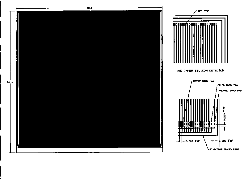
    The outer layer detectors have the same strip pitch and pad size, but the strips are longer. The detector measures 53 by 74.5 mm.

  2. Front End Electronics Layout The MVD front end electronics will be incorporated in a multichip module (MCM), most likely fabricated by Texas Instruments, using their HDI process (chip on board techniques are an alternative under current study). Figure 4 shows a layout of the current MCM design; the design will be finalized after tests and subsequent design changes of the individual front end elements. However, we do not envision radical changes in the general design. It should be noted that the HDI process prohibits leaving a window all the way down to the front end die - the MCM's are hermetically sealed. Consequently, it is not possible to bond the cable directly to the preamplifier bond pads. Furthermore, the risk from bonding directly to the front end die is large. A single bad bond would be cause to discard an entire MCM. Space constraints prohibit building large enough bond pads on the front end die to allow multiple bonding attempts. Also, bonding directly to the front end would make testing the MCM more difficult, without large pads which can be probed.

  3. System geometry Figure 5 shows the layout of one sector of the MVD central barrel. The scale is set by the size of the inner silicon detectors, which are 52mm long. The microcables are also shown in the figure connecting the detectors to the MCM's. Figure 6 shows the lavout a single detector-cable-MCM assemble This shows one of the longest cables. It should be noted that the apparent sections in the microcable are not in fact separate sections - the cable is one continuous cable, like the prototvpe which has been fabricated.

  4. Cable specifications We currently envision the bonds between the cable and detector and electronics to be achieved by ultrasonic wire bonding. Consequently, we would like to have a prototype cable without the windows required for welding. We envision making the wire bonds to the ends of the cable traces, so no special bond pads are necessary. However, 2mm of trace end is required to be exposed (not covered) allow for multiple bonding and probing operations .

    The capacitance of the cable can be up to 7-8 pF. This is determined by the performance of the preamplifier, which is optimized for 10 pF, and adequate up to 15 pF. The capacitance of the silicon strips is 3.5-4 pF.

    The standards for resistance of the cable are < 10 ohms, assuming Al traces. A copper trace option would imply a cable resistance in the range 100300 ohms. After further study, it has been decided that we should not put the ground grid on the back of the cables. The required shielding (the reason for this is clear from Figures 1 and 2) will be better provided by a solid metal sheet, either on the back of the cable and covered with a protective coating, or as a separate foil of aluminum.

    We have considered appropriate standards for protective coating of the microcables. Such a coating is definitely desirable, and we would like an additional 12 micron thickness of kapton. In fact,we find the prototype 12 micron kapton cable to be very thin and mechanically delicate for safe handling operations. With a 12 micron kapton cover, the mechanical strength should be adequate, and the thickness of the material still sufficiently small.

Operating Conditions for MVD

  1. Conditions of temperature, pressure, etc. are as follows: The MVD temperature will be controlled to 20 degrees C at tne silicon, and less than 40 degrees C at the electronics. This will be achieved by a slow flow of dry air over the silicon detectors (-1 m/sec) and a faster flow over the electronics (10-20 m/sec). It should be noted that the electronics cooling air will not flow across the wirebonds between MCM and cable, but will be contained in the plenum below the bonds. The MVD humidity will be controlled to 30-40% R.H. The radiation dose expected is several kRad per year.

  2. Mechanical tolerances The mechanical tolerances and stability requirements scale is set by the 200 micron pitch of the silicon strips. Not being a tracker, the MVD does not require few micron resolution. The mechanical conditions for the cables are relatively straightforward. The cables will be constrained at each end by the glue joint, and there is not a stringent strain-relief requirement inbetween. The worst case bend of the cable has a bend radius of 2mm, this occurs for the top inside silicon detector.

  3. Signal frequency The signal frequency transmitted along the cable is 25 MHz; the silicon rise time is 15 ns.

Production Requirements

  1. Cable connections The cable connections (most likely ultrasonic wire bonding) will be made using assembly fixtures for positioning. We envision the bonding will be done commercially, using a wire-bonding apparatus in a clean room. We do not expect bonding to be done "on the spot" at either Los Alamos or Brookhaven . The bond strength of an Al to Al wire bond should be equal to or greater than 8 grams. The failure mode is specified to be breaking of the wire rather than pulling up of the bonds.

  2. Cable bend radius Though the smallest bend radius of the cable during MVD operation is 2 mm, it is necessary to have a smaller bend radius specification for handling safety during assembly. Ideally, the cable should be able to withstand folding into an accordion shape. A bend radius equal to or less than 250 microns will be acceptable.

  3. Cable maintainabilityThe cable traces should be covered to simplify handling procedures. The cables, traces, and bonds should be stable (mechanically and electrically) for 10 years. The environment will be temperature and humidity controlled, as specified above. 2mm trace ends must be exposed to allow 2 probe areas and at least three wire bonds to be made. The cables, traces and bonds must be compatible with epoxy adhesives.

Last Updated: 1/3/96