PHENIX.ONCS.TN.7.1
(file:mvd_daq.ps)
Jehanne Simon-Gillo, Tom Carey, Tom
KozlowskiLos Alamos National
Laboratory
March 3, 1995
The Multiplicity Vertex Detector sub-system is planning to test a full silicon
assembly during the summer of 1995. This implies an assembly of a silicon
detector (either pad or strip), kapton cable, and prototype front-end
electronics designed and constructed at Oak Ridge National Laboratory. We would
like to incorporate a data acquisition system into our test set-up. The entire
system (detector through DAQ ) will first be used in the lab, starting June
1995, and then in a beam test. The beam test will either be held at LAMPF in
September 1995 or at the AGS in early 1996. The beam test will involve
collaborators from Los Alamos, University of California @ Riverside and Oak
Ridge National Laboratory.
The primary goal of this test is front-end electronics characterization. The
aims are as follows:
- - Test behavior of prototype electronics in "real" environment
- - First tests of AMU/ADC
- - First tests of prototype heap manager
- - Measure signal to noise
- - Measure correlated noise
- - Dynamic range of pre-amp
- - Test MVD shielding of electronics
- - Test variable capacitance of different length kapton cables . (This test
implies two separate silicon assemblies.)
- - Characterize calibration circuitry
- - Characterize analog (discriminator) sum circuitry
The set-up for the lab/beam tests is shown in Figure 1. The silicon detector
will be attached to the front-end electronics via a kapton cable. The digital
data will exit the FEE in parallel on a ribbon cable to an external FIFO. This
FIFO will be located close to the silicon assembly. The data is then piped out
of the FIFO and to the DAQ. For the beam tests, this may imply a significant
distance for the data to be transferred from the FIFO to the DAQ, if the latter
is located entirely in the counting house.
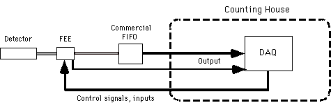
Figure 1. General set-up of laboratory and beam tests.
The FIFO should be a commercial VME or CAMAC module, such as is offered by CES
or LeCroy; the actual model has not been defined and is open to discussion, but
ones needs to be chosen soon in order to freeze specification of the FEE-FIFO
protocol.
There is also analog data which exits the FEE via coaxial cables and goes
directly to the DAQ. Means for synchronizing it to the associated digital data
have not yet been considered.
Configuration, initialization, and control of the FEE will be done through a
serial link which is not yet fully specified.
The data acquisition system will have to manage several inputs and outputs for
the FEE. A drawing of the front-end board is shown in figure 2. A description
of the signals are listed below.
- 9MHz clock (on ribbon cable)
- 36 MHz clock (on ribbon cable)
- Level 1 ACCEPT (on ribbon cable)
- Triggers conversion and readout from FEE to FIFO.
- Serial link (on ribbon cable)
- Includes serial in, serial readback, serial latch, and serial clock.
- The serial in includes discriminator threshold and test enable (controls
calibration circuitry)
- Mode bits (on ribbon cable)
- This tells the heap manager what commands to execute and includes
variable time reset. (3 bit)
- Analog ground (wire braid)
- Digital ground (on ribbon cable or wire braid)
- Power to FEE (on wirebraid)
- Calibration input (on coaxial cable)
- This is a voltage or pattern, defined via the serial link..
- Detector ground (on wirebraid)
- Detector bias (on wirebraid)
Note: Items a through e and possibly g will be on the same ribbon cable.
- Parallel data + "handshake" to external FIFO (ribbon cable) (10bit)
- Clock and FIFO status information to external FIFO (ribbon cable)
- Serial link readback ( on ribbon cable described in section 4.1)
- 4 separate analog sums (on coaxial cables)
- Want the ability to voltage sum after individual read-out.
Note: Items a and b will be on the same ribbon cable.
We are interested in three types of data output: Internal and external ADC,
external TDC and digital scope. The digital scope could be used to monitor
individual AMU cells and output from individual pre-amps. This is not shown in
Figure 2, but these options will be on the TGV 32 channel prototype which will
be available for beam tests in early 1996. The 4 analog sums will get split to
the digital scope, ADC and TDC. The digital information from the AMU/ADC will
go to the DAC for analysis after the commercial FIFO.
We expect trigger rates in the 100Hz - 10Khz range, with 1Khz typical. A
typical event size should be less than 1KB, although the digital scope may
produce up to 8KB "frames" for each of 8-10 channels.
We are interested in a data acquisition system with the following
characteristics:
- a) Provide input and control signals as described in Section 4. Real time
monitoring of detector currents is desirable. Possible control of detector bias
supplies is also desirable.
- b) Ability to read-out commercial FIFO, ADC, TDC, digital scope on an
event-by-event basis (section 5).
- c) Ability to start/stop runs at user's discretion.
- d) Allow calibration as well as data taking modes, with the possibility of
calibration events interleaved with "normal" data events.
- e) Include on-line histograming package.
- f) Need to be able to manipulate data in histograms- fits, averages,
subtractions, etc.
- g) Include data storage, such as writing to 8mm tape. Would also like to
save outpu from digital scope via GPIB interface.
- h) Robust and practical enough to be used in lab tests in summer then beam
tests.
- I) User-friendly.
- j) Can utilize as much of existing equipment as possible.
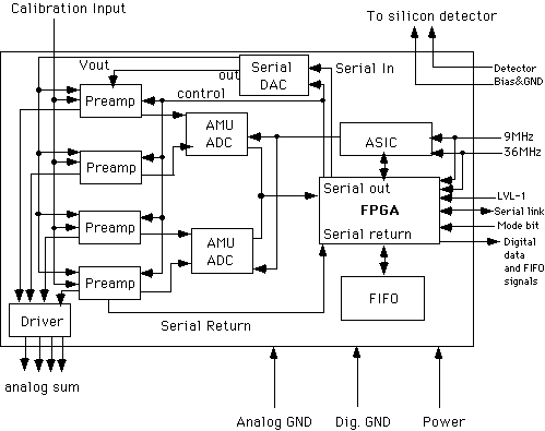
Figure 2. Diagram of front-end electronic testboard