 Send Mail to Jehanne Simon-Gillo
Characterization and quality control of silicon microstrip detectors with an infrared diode laser system
S. Shaheen, J. Boissevain, W. Collier, B.V. Jacak, J.S. Lock, P. Roybal,
J. Simon-Gillo*, W. Sondheim, J.P. Sullivan and H. Ziock
Physics Division, MS D456, Los Alamos National Laboratory, Los Alamos, NM 87545, USA
Published in NIM A 352 (1995) 573-578.
PHENIX-MVD-95-1
PHENIX Note #122
Abstract
A system using a 1064 nm infrared diode laser has been developed to characterize silicon microstrip detectors. The spot size from the diode has been optically collimated to 25  m so that strips can be irradiated individually. Results from diagnostic tests such as strip-to-strip variations, attenuation length along a strip, angle of incidence and charge sharing studies are presented. An affordable, computer-controlled system has been built to test many silicon sensors prior to final assembly of the detector.
1. Silicon vertex detector diagnostics
The design and construction of a silicon vertex detector requires the ability to efficiently characterize prototype silicon sensors and front-end electronics, as well as the final assemblies prior to installation in the full detector. It is important to be able to determine whether a pixel or strip is alive, if a bond (between silicon and electronics, for example) is properly working or whether an electronics channel is functional and giving the expected response. A test station was developed which utilizes an infrared laser diode to characterize silicon sensors and front-end electronics. Diagnostic tests including strip-to-strip uniformity, strip attenuation length and capacitive coupling studies can be performed.
The benefit of using a simple, automated testing station is the provision of fast quality control for a large number of silicon sensors which can be managed by non-experts. The system is flexible and can be used with any silicon strip sensor, regardless of strip pitch, size of detector or output response. A quality control station has been designed to scan several silicon assemblies simultaneously to judge performance prior to final assembly.
This group is involved in designing and constructing a silicon multiplicity vertex detector for PHENIX. The primary goal of the PHENIX experiment at the Relativistic Heavy Ion Collider (RHIC) being constructed at Brookhaven National Laboratory is to detect a new phase of matter, the quark-gluon plasma and investigate its properties. The Relativistic Heavy Ion Collider will be capable of accelerating gold ions to 100 GeV/nucleon per colliding beam and is planned to be completed in 1999. PHENIX will employ silicon sensors close to the collision point to provide event characterization, a centrality trigger, the collision vertex position along the beams, and a search for fluctuations in charged particle distributions. The design of the MVD and a description of the front-end electronics are described elsewhere [1, 2].
2. Laser diode station
The laser diode system allows for both the characterization of the sensors and electronics and the testing of the assemblies before installation. A 1064 nm laser diode, Laser Diode Incorporated model QP106 [3], mimics the passage of one to several minimum ionizing particles (MIP) through the silicon sensor. The choice of a wavelength near the silicon band gap energy insures nearly uniform creation of charge along the pathlength of the light in the silicon sensor [4]. The diode has a maximum power output of 85 mW and can produce light pulses with rise times less than 1 ns. It requires a voltage biasing of ~ 30 V and a 4.5 V pulsed input. The laser is coupled to a single-mode l m long fiber, terminated with a focussing lens to yield a spot diameter of ~ 25 m with a focal length of l cm [5]. The final power output from the coupling fiber is 390 nW, which categorizes the system as a Class 1 laser and exempts it from complicated safety requirements. In addition, the total cost of the laser and optics is less than $5000 (US).
Fig. 1 illustrates the setup of the testing station. The sensor is fixed to an x-y stage. Stepper motors, with a position resolution of 5 m, are attached to each axis and driven by a Unidex stepper motor controller [6]. The infrared laser beam is directed perpendicular to the sensor via an optical fiber. The output voltage of the sensor and front-end electronics is measured by a Tektronix DSA602A oscilloscope. A Macintosh running LabVIEW [7] provides control of the stepper motors and records and analyzes the detector response data. The LabVIEW environment is an object oriented programming language that can be used to handle all interfacing, control and analysis of data; the GPIB interface standard is used for all communications.
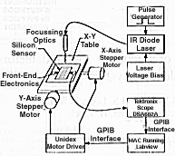
Fig. 1. Setup of the laser diode test station.
The results presented in this paper were obtained with a single-sided 300 m OPAL silicon wafer, with strip and readout pitch of 25 and 50 m, respectively [8, 9]. The front-end electronics used in this work is a CMOS charge sensitive preamplifier-shaper with a peaking time of 200 ns and a conversion gain of ~ 75 mV/fC for a 0 pF detector capacitance [10]. Fig. 2a shows the response of the silicon sensor and associated front-end electronics to 60 keV  s from an 241Am source (l MIP ~100 keV). Fig. 2b shows a sample output pulse when irradiated with the infrared laser; the amount of deposited charge from the laser corresponds to the passage of 1 MIP through the silicon.
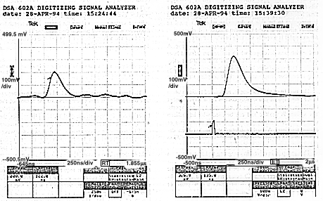
Fig. 2. (a) (left) Response of OPAL sensor using 200 ns peaking time electronics to 60 keV s from 241Am source. (b) (right) Response of the same silicon assembly to laser diode as measured by the DSA in averaging mode. Input pulse to laser is shown below the detector response.
The silicon sensor is essentially a series of p-n junctions. The induced photocurrent in a p-n junction is directly proportional to the incident photon flux at a given wavelength [11]. Fig. 3 shows sensor output voltage versus laser bias voltage. Two regimes are seen before the amplifying front-end electronics reach saturation. This is due to the behavior of the infrared diode laser, which has two modes of operation [12]. Below a turn-on voltage of 25.8 V, the diode undergoes spontaneous emission. Above the threshold, stimulated emission begins and the device starts lasing. In the spontaneous emission case, the output wavelength varies with applied voltage and is greater than the rated 1064 nm. Once the diode begins lasing, the output is a constant 1064 nm. Region II of Fig. 3 displays the linearity of photon flux to output voltage. In order to maintain a constant wavelength, the operating voltage must be chosen from the stimulated emission regime. Furthermore, the absorption length of silicon is a function of the wavelength of the light incident upon it [11]. The 1064 nm laser falls on the absorption edge for silicon, which has an energy gap of 1.12 eV at room temperature. This results in a high sensitivity of the absorption length to the incident wavelength. Therefore, it is also important to operate the diode laser above the threshold voltage to ensure a reproducible absorption length. An operating voltage of 28.0 V was chosen for these tests.
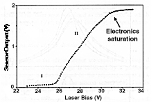
Fig. 3. Sensor response as a function of laster bias voltage. In region I, the laser is emitting via spontaneous emission. Lasing occurs in region II and the output is linear until the amplifying electronics saturate.
The output intensity of the laser varies with changing temperature [12]. This results in a silicon sensor response that is also dependent upon temperature. In the temperature range of 20 to 30 C, the slope of this dependence has been measured to be -0.014
  0.003V/C. This linear scaling with temperature can be used to correct absolute measurements of the silicon sensor output. At a given temperature, the output intensity of the laser is stable to within 3%.
3. Characterization of silicon sensor with laser testing station
3.1. Angle of incidence studies
Using a laser as a diagnostic tool introduces effects such as reflection, refraction and absorption into the analysis. Multiple internal reflections are established inside the silicon sensor because of the reflective aluminum backing and the SiO2-Si boundary. These change the effective path length, which is important in understanding how much of the infrared light is absorbed. The angle at which the beam enters the silicon also affects the pathlength. It is necessary to fully understand these effects in order to use the laser as a tool to simulate charged particles passing through the sensor.
The reflection coefficient for the boundary between two different layers is given by (n1-n2)2/(n1 + n2)2, where n1 and n2 are the complex indices of refraction in the two layers [11]. The real part of n is the familiar index of refraction. Values for Si, SiO2 and air are 3.6, 1.5 and 1.0, respectively [12]. These values give a reflection coefficient of 0.04 for the air-SiO2 boundary, 0.17 for SiO2-Si and 0.32 for air-Si. Aluminum is nearly completely reflecting at 1064 nm. The complex part of the index of refraction, also referred to as the extinction coefficient, determines the absorption of light by the material.
The intensity follows an exponential decay, given by  =
oe-
=
oe- d,
where o is the original intensity,
d is the distance through the material and
is the absorption coefficient [13]. is defined by k, the extinction coefficient, and
d,
where o is the original intensity,
d is the distance through the material and
is the absorption coefficient [13]. is defined by k, the extinction coefficient, and  , the wavelength:
  . For silicon, k is several orders of magnitude smaller than the real part of n and can be ignored for refractive and reflective studies.
For refraction of transmitted light through a boundary, the change in angle is given by Snell's law: n1 sin  l = n2 sin 2, where is the angle with respect from the normal to the surface. The angle of the beam is therefore reduced when going from a low index material to a higher one, such as silicon. For example, when 1 ~ 90 (an incident beam that grazes the silicon surface), 2 = 16.6. This is the maximum angle at which the beam can pass through the silicon, and places a limitation on the use of the laser for simulating high angle particle trajectories. Furthermore, at such shallow angles of incidence the projection of the laser spot on the silicon surface becomes oblong.
Measurements were carried out to investigate the feasibility of using the laser to mimic particle trajectories at angles of incidence other than normal to the silicon sensor. The technique for doing this is to adjust the angle of the laser and then reposition its height in order to maintain focus on the surface of the sensor. The laser is used to scan horizontally across the sensor, perpendicular to the strips. Readout is taken from one strip only, and the sensor is scanned over a range of 400 m on either side of this strip. Figs. 4a and 4b show plots of laser position versus output voltage for normal, 30 and 45 angle of incidence. Maximum output voltage is detected near the center, which is the readout strip. The voltage is non-zero away from the readout strip because of crosstalk and charge sharing. Output variations are due to reflections off the aluminum strips at the surface of the sensor. Different angles of incidence have only a subtle effect on the shape of the curves due to the limiting effect of refraction at the silicon boundary. The pathlength increase in only 2% for 45 over 0, disregarding reflection effects.
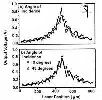
Fig. 4. Measured sensor response as a function of laser position. (a) Response at normal and 30 incidence. (b) Response at normal and 45 incidence.
Simulations were performed to convince ourselves that we could correctly model the response of our silicon detector as well as to understand how optical phenomena, such as refraction, reflection and absorption, effect the laser's ability to mimic a particle with some angle of incidence. A calculation of charge collected versus laser position was done with adjustable parameters such as angle of incidence, absorption length and whether or not to use reflection or refraction. For the calculations presented, a value of 1.1 mm is used for the absorption length of light in silicon [4, 14], and both reflection and refraction are considered. Fig. 5a shows the results with four angles of incidence overlaid: normal, 30, 60 and 90 (grazing angle). As in the actual measurement, the difference between the curves is not large. Fig. 5b shows the simulation without the limiting effects of refraction. The simulation shows that higher angles of incidence significantly change the structure of the curve. The peak is decreased and shifted, and the curve is broadened. These changes are also seen in the full simulation (Fig. 5a) but to a much lesser extent.
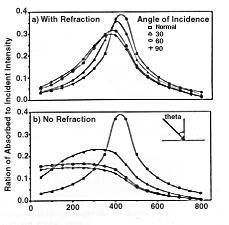
Fig. 5. Calculated response of sensor as a function of laser position for angles of incidence, normal, 30, 60, and 90 . (a) includes the effect of refraction and (b) neglects the influence of refraction.
Calculations were also done to study varying absorption length and the effect of internal reflections in the silicon. As the absorption length is decreased or internal reflection is included in the simulations, the absorbed intensity increases. Thus, the distributions in Fig. 5 would have similar structure, but higher absolute values for the absorbed intensity. Neither internal reflections nor varying absorption length limit angle of incidence measurements, but refraction prohibits the simulation of particles with angles of incidence other than normal. The following sections will demonstrate the laser station's ability to effectively characterize silicon sensors when the laser is at normal incidence.
3.2. Fine structure of silicon strips
When the laser is incident upon one of the aluminum strips on the surface of the sensor, a fraction of the photons are reflected back. If the width of the aluminum strips is an appreciable fraction of the laser spot size, the variation in the output voltage as the laser is scanned across the sensor is maximized. This allows the study of the sensor fine structure, the focussing of the laser on the surface of the sensor, and an estimation of the laser spot size.
Fig. 6 is a series of plots of output voltage versus horizontal laser position. The sensor was scanned perpendicular to the strip orientation at approximately 5 m intervals. Each plot displays a scan with a different laser height. Variations in the output voltage are greatest when the spot size of the laser is a minimum at the surface of the sensor, corresponding to the laser being in focus. From the plots, a focal length of 9.7 mm was determined. The laser was positioned at this height for all measurements.
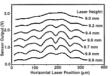
Fig. 6. Sensor response as a function of IR laser horizontal position when the diode is positioned at various heights above the sensor. The optimal resolution is obtained at a height of 9.7 mm.
The width of the aluminum strips is 10 m. The ratio of output voltages when the laser is centered on an aluminum strip to when it is centered directly on the silicon is 0.45/0.77. With this information, the spot diameter of the laser was calculated. The laser intensity is not incident upon the surface uniformly [15]. Instead, it has a maximum at the center and falls off as a Gaussian distribution. The radius of the laser spot is defined as the distance at which the intensity is 1/e2 the central intensity; the spot diameter is 253 m.
3.3. Capacitive charge division
The strips in the silicon sensor are capacitively coupled to each other. When charge is collected by a particular strip, charge is also induced in the adjacent strips as a result of the geometry of the silicon sensor [16]. This is true for charge creation by either ionizing particles or laser irradiation. The infrared laser provides a means of studying the capacitive charge sharing. Normalized to the output voltage from the strip upon which the laser is incident, the response of the strips that are adjacent one away, and two away, are 0.4 and 0.2, respectively. It is possible that internal reflections inside the silicon sensor put light into neighboring strips, increasing the charge sharing measured with the laser. The electronic crosstalk is inherent to the amplifying electronics and is less than 1% [10].
3.4. Attenuation length and strip-to-strip uniformity
The laser diode test station is an efficient tool for determining the output voltage along the length of a strip, an important step in characterizing the response of a particular sensor. Fig. 7 shows the results of a 2.0 cm scan along the length of two strips, at 0.2 cm intervals. The strips are adjacent strips, and since adjacent strips are read out at opposite ends of the detector, an increase in the laser position corresponds to approaching the bonding pad of strip (a) and moving away from the bonding pad of strip (b). The scan was started near the center of the sensor and ended near the edge of the silicon active area. The response along both strips is uniform.
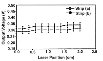
Fig. 7. Sensor response as a function of laser position along the length of two strips. As distance increases, the laser moves closer to the bonding pad of strip (a) and farther from the bonding pad of strip (b). Error bars represent magnitude of the measured strip-to-strip uniformity.
Strip-to-strip uniformity measurements have also been performed with the laser diode. The sensor is scanned from one strip to the next, keeping the position along the length of the strips fixed. The response measured from seven strips varied less than 6%. This enables one to characterize detector qualities such as nonuniform strip width.
4. Conclusions
An affordable, computer-automated test station using a 1064 nm laser diode has
been used to test silicon sensors and associated front-end electronics. The infrared diode mimics the passage of charged particles through the silicon. Diagnosotic tests such as strip-to-strip variations, signal attenuation length along the strip and capacitive coupling measurements can be performed in a quick and easy fashion. Due to the influence of refraction, the laser system is not an efficient tool to study the effects of varying angle of incidence. The automated nature of the test station allows one to test large numbers of silicon sensors quickly. This allows the possibility of quality control prior to final assembly of a silicon detector.
References
- PHENIX Conceptual Design Report, Brookhaven National Laboratory, 1993.
- J.S. Lock, et al., Nucl. Instr. and Meth. A 345 (1994) 284.
- Laser Diode, Inc., High Power Laser Components, 1130 Somerset St., New Brunswick, NJ 08901.
- Y. Tomita, et al., Nucl. Instr. and Meth. A 270 (1988) 403.
- OZ Optics, LTD., Unit 2-244 Westbrook Rd, West Carlton Industrial Park, Ontario, Canada, KOAlLO.
- Unidex III Stepping Motors, Aerotech, Inc., 101 Zeta Drive, Pittsburgh, PA, 15238.
- LabVIEW, National Instruments, 6504 Bridge Point Parkway, Austin, TX 78730-5039
- P.P. Allport, et al., Nucl. Instr. and Meth. A 324 (1993) 34.
- Micron Semiconductor Inc., 126 Baywood Avenue Longwood, Florida 32750
- C.L. Britton, Jr., et al., IEEE Nucl. Sci. Trans. 41 (1994) 352.
- H.J. Moller, Semiconductors for Solar Cells (Artech House, Boston, 1993).
- S.M. Sze, Physics of Semiconductor Devices, 2nd ed. (Wiley, New York, 1981)
- M.V. Klein, Optics (Wiley, 1970).
- E.D. Palik, Handbook of Optical Constants of Solids (Academic Press, Inc. 1985).
- J.P. Machewirth, The Photonics Design and Applications Handbook (1988).
- J.B.A England, et al., Nucl. Instr. and Meth. 185 (1981) 43.
Corresponding author: J. Simon-Gillo