 Send Mail to Jehanne Simon-Gillo
Air cooling of front-end electronics for silicon detectors in a collider experiment
J.S. Lock, E. Bertson, J. Boissevain, D.J. Clark, W. Collier, R. Hammock, B.V. Jacak, A. Morgan, P. Roybal, S. Shaheen, J. Simon-Gillo* and J.P. Sullivan
Physics Division, MS D456, Los Alamos National Laboratory, Los Alamos, NM 87545, USA
Published in NIM A 345 (1994) 284.
PHENIX Note #101
PHENIX-MVD-94-1
We have investigated the feasibility of using room temperature air to cool front-end electronics for silicon microstrip and pad detectors in a collider experiment. Advantages of air cooling include minimal material in the path of the particles and no potential of coolant spills in the silicon region. A prototype cooling system was tested with heat provided by flat resistive heaters. Heat loads from 1 to 27 mW/channel were studied, making the results applicable to various silicon detector systems. The measurements are compared to cooling system performance predictions. A set of simple equations has been identified and tested which reliably describe the lab setup.
1. Silicon multiplicity vertex detector
The primary goal of the PHENIX experiment at the Relativistic Heavy Ion Collider (RHIC) being constructed at Brookhaven National Laboratory is to detect a new phase of matter, the quark-gluon plasma and investigate its properties. The Relativistic Heavy Ion Collider will be capable of accelerating gold particles to 100 GeV/nucleon per colliding beam and will be completed in 1998.
PHENIX will employ silicon sensors close to the collision point to provide event characterization, a centrality trigger, the collision vertex position along the beams, and a search for fluctuations in charged particle distributions. The multiplicity and vertex detector (MVD) has silicon strip detectors arranged in two concentric barrels around the beam pipe in the center of PHENIX, and endcaps consisting of a single layer of silicon pad detectors. The silicon barrels consist of 300  m thick AC-coupled FOXFET (field oxide field effect transisitor) silicon sensors. Each detector has 256 strips at 200
  m pitch perpendicular to the beams. The barrels have six azimuthal sectors of twelve detector sensors along the beam direction, for a total length of 64 cm. The single-event coverage about mid-rapidity is five units in pseudorapidity (
 ) for the inner barrel layer and four units for the outer layer; however, the
  coverage for event-averaged quantities is extended due to the variation of the vertex position along the direction of the colliding beams.
The disk-shaped endcaps, which comprise pads ranging in size from approximately 2 X 2 to 5 X 5 mm2, are positioned in z at -35 and +35 cm. One pad endcap is composed of 12 trapezoidal "sectors", each manufactured from a 4 in. wafer. The  segmentation is more than adequate for fluctuation studies, and pulse height analysis allows the unfolding of multiple hits in one pad. The azimuthal segmentation and full azimuthal coverage allow a high sensitivity search for fluctuations in the particle multiplicity. The highest channel occupancy for central events is ~ 0.46 for dNch/d
 = 1000. The total channel count in the barrels and endcaps is 28 672 and 6 144, respectively [1].
The silicon sensors operate at the ambient enclosure temperature and are connected to the electronics by kapton cables. This physical separation provides thermal isolation of the silicon and eliminates the need to cool the sensors, thus minimizing vibration effects. The position stability of the electronics is less critical than that of the sensors, which are only coupled to air flow-induced motion via the flexible kapton cables. The electronics are the main heat source in the system, and thus determine the cooling requirements.
The silicon detector system will utilize custom designed front-end electronics fabricated using a 1.2  m CMOS process. As the silicon pads range in capacitance from 10 to 25 pF, and the silicon strips with cable are of order 10 pF, the same front-end electronics can be used for both [1,2]. The chain of front-end electronics includes a preamplifier/shaper chip, analog memory plus digitization (AMU/ADC circuit), FIFO (first in-first out), optical fiber driver, and "heap manager", all of which are mounted onto a Multi-chip module (MCM). The MCM is fabricated using the High Density Interconnect process from Texas Instruments [3]. The preamp/shaper chip will have 256 channels, a shaping time of ~ 60 ns, dynamic range of 8 minimum ionizing particles, signal to noise of 20:1 and a gain of 41 mV/fC. The expected preamp power dissipation is ~ 1 mW/channel. The analog memory unit (AMU) is a switched capacitor array with simultaneous read/write capability to pipeline the data pending a low level trigger decision. Each channel has its own ADC circuit and a FIFO of at least two registers to store the data for readout. The silicon detectors will provide information on the charged particle multiplicity for triggering via a sum of channels above threshold. Control of the AMU, ADC and FIFO is provided by a heap manager controller, a field programmable gate array. The total power dissipation of the multi-chip module is foreseen to be less than 5 mW/channel, leading to a total heat load of 174 W for the silicon detector. The silicon strip electronics are mounted at the bottom of the silicon barrels, minimizing the material thickness in the direct path of the PHENIX active area to avoid producing conversion electrons. Fig. 1 shows a schematic layout of the barrels, endcaps and front-end electronics.
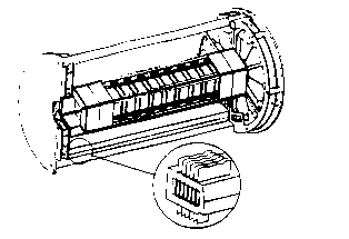
Fig. 1. Layout of the silicon microstrip and pad detectors in the MVD. The top four sectors of the outer barrel contain no silicon in order to minimize the amount of material in the particle path. The front-end electronics are connected to the silicon via kapton cables and are located at the bottom of the detector. A blowup of this region displays how the multi-chip modules aid in defining the plena for channeling the cooling air. Kapton cables exit out of the top of the plenum and interface cables exit out the bottom.
The MVD resides in an enclosure which opens in a "clam-shell" fashion to allow installation around the beam pipe. The half-cylinders are covered on each side to provide environmental isolation of the MVD and mechanical protection. Each row of 12 barrel MCMs forms one side of an individual plenum to provide a path for the cooling air and electrically isolate the multi-chip modules. Each plenum is 2.0 cm wide by 64 cm long, dictated by the size of the 12 adjacent MCMs. The endcap MCMs are enclosed by a curved plenum, similar in aspect ratio, enclosing six MCMs. Air flows along both sides of the MCMs, although the heat transfer to the cooling air is largely from one side of the MCMs as the other side is covered by polyimide, which has a poor thermal conductivity. The barrel multi-chip modules are grouped together in each half-cylinder and surrounded by a plena of low Z-material such as Rohacell foam [4] to further channel the cooling air. The total heat load in one silicon strip plenum is 15.4 W and the total heat load in one silicon pad plenum is 7.7 W.
2. Conceptual design of cooling system
Air cooling is desirable as it eliminates the possibility of coolant spills in the region of the silicon and implies a simpler and lower-mass system, miminizing the material in the particle path. The cooling system must keep the electronics at less than 50 C, where CMOS components become temperature sensitive. The design goal is to keep the electronics below 40
 C to allow for a safety margin. The cooling system must eliminate temperature fluctuations with time to maintain the required position accuracy of the detector elements. Of course, the flow of cooling air must not itself affect the positioning of the sensors by introducing vibrations; we ensure this by limiting the air flow to the electronics region.
Fig. 2 shows the air flow distribution supplying the plena for the barrel and endcap silicon inside an enclosure half. The air is driven into the enclosure halves by a fan and circulated through a heat exchanger located outside of the system; dry air is circulated over the electronics in order to avoid condensation problems. Air enters from one side, at the bottom of the enclosure, and is split into two streams. One stream flows through the group of plena holding the barrel MCMs, and the other passes through the half-circular plenum covering the endcap MCMs. This air then flows to the other side of the enclosure to cool the MCMs of the other endcap. The path from one side of the enclosure to the other is inside one of the graphite composite tubes serving as a structural strut. After passing along the MCMs of the other endcap, the air then joins the barrel cooling air and exits the enclosure to be cooled and recycled or vented outside of PHENIX. The MVD outer enclosure provides humidity control and thermal isolation of the cooling air inside the plena making it possible to use chilled cooling air, providing a safety margin for the MVD cooling needs.
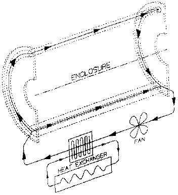
Fig. 2. Cutaway view of the silicon support and enclosure showing the entry and exit path of the cooling air. Arrows indicate the direction of the air flow.
3. Measurements and expected cooling system performance
The MVD air cooling conceptual design was tested in the laboratory with a plenum made of phenolic (a paper/resin composite) and insulating foam. The thermal load of the electronics was provided by flat resistive heaters from Minco [5] arranged in the geometry planned for the MCMs. The heaters were powered to simulate plenum heat loads from 3 to 83 W (1-27 mW/channel). Six sensors recorded temperature changes at various points along the length of the plenum [5]. The dimensions of the lab plenum were 5.5 X 64.0 X 0.8 cm, representing the geometry of the MCMs at the time of the laboratory measurements. A large aspect ratio (plenum width/height) was chosen to minimize the hydraulic diameter, directly proportional to the Reynolds number, in an attempt to simulate laminar flow [6]. Fig. 3 shows the setup of the air cooling prototype. Five different air velocities were studied ranging from 4.8 to 14.4 m/s. A Dwyer VFC 5 in. flowmeter, capable of measuring 2.5-25 SCFM, was used to measure the air flow rate. The air velocity was determined with a Sper Scientific 840003 anemometer. A Centrimax CX29AG fan was used to produce the cooling air.
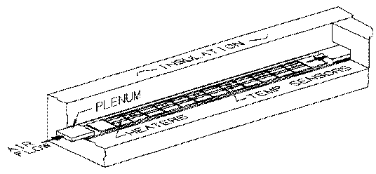
Fig. 3. Layout of the air cooling system prototype.
Three different quantities were measured as a function of heat load and air velocity. The maximum temperature recorded by the sensors when the resistors are being heated corresponds to the maximum temperature reached by the multi-chip modules. This quantity is essential in determining whether it is possible to use air cooling to maintain the temperature of the front-end electronics at less than 40 C. The heating of the air as it flows through the plenum,
  T 1, is measured as the difference between room temperature and air temperature at the plenum outlet. In addition to illustrating the general behavior of the cooling prototype,
  T 1 enables the confirmation of flow rate, as will be shown below. If chilled instead of room temperature air is being used,
  T 1 is important in studying the range of temperatures reached within the plenum to avoid condensation on the outside of the detector enclosure.
  T 2 is the temperature difference between the air and the prototype MCMs, namely the difference between the average
  T 1 and the average temperature change recorded by the six sensors when the resisitors are heated. As will be shown, it also can be used to calculate the heat transfer coefficient. Both
  T 1 and
  T 2 can be compared to the predicted cooling system performance to identify a set of equations describing the cooling design. This greatly simplifies prototype tests should there be changes in the front-end electronics specifications. These basic equations can be applied to the conceptual design of other front-end cooling systems.
The following heat transfer equations were used for cooling performance predictions for a system experiencing heat loss by convection [6]. Assuming uniformly distributed heat, the temperature difference between the electronics and the air can be expressed as:
 T 2 = Q/Ah X (l/h), (1)
where Q is the heat load (W), Ah is the heated area in the plenum (333 cm2), and h is the heat transfer coefficient (W/ C cm2). From laboratory measurements of
  T 2, one can determine h and compare to predictions of the heat transfer coefficient. The heat transfer coefficient can be calculated as follows:
h = JC pG(CpMu/K)-2/3 (2)
where J is the Colburn factor, a quantity which can be derived from the Reynold's number (NR) The Reynold's number represents a measure of the type of flow a system is experiencing, laminar or turbulent. Laminar flow is advantageous as it implies a minimum disturbance to the components being cooled and thus reduces vibrational effects. Turbulent flow is desirable as it is more effective in transferring heat from the surface components to the cooling air. The actual transition between laminar and turbulent flow is historically not well understood and poorly defined. In this case, J was calculated for both laminar and turbulent flow and set to a value (0.0038) which could be indicative of either; therefore, J makes no assumption on the type of flow in the system. Cp is the specific heat of air (l J/g C), G is the mass flow per unit cross sectional area per unit time (g/s cm2), Mu is the viscosity of air (1.8 X 10⁻⁴ g/s cm), and K is the thermal conductivity of air (2.6 X 10⁻⁴ W/cm
 C). The heat transfer coefficient can also be expressed as:
h = G4.8 X 10-3. (3)
Knowing G and h, the change in the cooling air temperature can be calculated:
 T 1 = Q/(GAc Cp) (4)
where Ac is the cross sectional area of the plenum (4.4 cm2).
4. Results and conclusions
Fig. 4 shows the measured and predicted  T 1 as a function of power for five different air velocities. For the case of the MVD, in which the maximum heat load per plenum is 15.4 W,
  T 1 ranges from 2.0-5.3
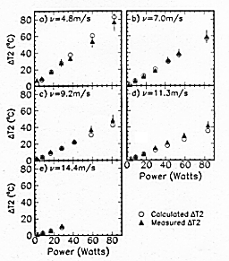
 C as the air velocity is increased from 4.8 to 14.4 m/s. The temperature difference between the cooling air and electronics as a function of power for various air velocities is shown in Fig. 5. At a heat load of 15.4 W,
  T 2 ranges from 5.2-15.8
 C as the air velocity is increased from 4.8 to 14.4 m/s. The determination of
  T 2 enables the comparison between measured and predicted heat transfer coefficients as a function of air velocity, shown in Table 1. The measured heat transfer coefficient is determined from an average of the values attained from each heat load within a given air velocity setting. The predicted heat transfer coefficient is calculated from Eq. (2).
Velocity
[m/s] | Predicted h
[W/ C cm2] C cm2] | Measured h
[W/ C cm2] C cm2] |
|---|
| 4.8 | 0.0030 0.0002 0.0002 | 0.0028 0.0005 0.0005 |
| 7.0 | 0.0044 0.0002 0.0002 | 0.0047 0.0007 0.0007 |
| 9.2 | 0.0057 0.0003 0.0003 | 0.0048 0.0008 0.0008 |
| 11.3 | 0.0071 0.0004 0.0004 | 0.0066 0.001 0.001 |
| 14.4 | 0.0090 0.0005 0.0005 | 0.0072 0.002 0.002 |
Table 1: Comparison of measured and predicted heat transfer coefficients.

Fig. 4. The heating of the air flowing throught the plenum.  T1, as a function of power for various velocities (
 ). Both the calculated and measured values of
  T1 are shown.

Fig. 5. Temperature difference between the electronics and the air versus power for various velocities ( ). The
  T2 from measurements and predictions are included.
The trends displayed by  T 1 and
  T 2 give us confidence in our measurements and predictions. As expected, the heating of the air increases as the heat load is increased and the air velocity is decreased. The temperature difference between the cooling air and the electronics behaves accordingly, with
  T 2 increasing with increasing power and decreasing air velocity. Good agreement is observed between the predicted and measured values of the heat transfer coefficient,
  T 1, and
  T 2. These predictions reliably describe our lab. setup, enabling the use of these equations to simplify future cooling studies should changes in the front-end electronics specifications occur. Other groups designing cooling systems for front-end electronics may find these basic equations useful.
Fig. 6 shows the maximum temperatures reached by the MCMs as a function of power for different air velocities. As expected, the maximum temperature attained increases with increasing power and decreasing cooling air velocity. With a heat load of 15.4 W/plenum, temperatures less than 42.1 C can be maintained with air velocities of 4.8 m/s and temperatures less than 34.2
 C with air velocities of 7 m/s; the maximum temperature reached for an air velocity of 14.4 m/s is 29.2
 C. The results indicate that it is possible to air cool the MVD electronics, maintaining their temperature at our design goal of 40
 C. This determination will enable the design of a simpler, lower-mass system, with no coolant leak hazards. The low flow rates along with the separation of the cooling system from the silicon sensors minimizes the vibration effects in the detectors. The range of heat loads and air velocities studied makes our results applicable to various detector systems.

Fig. 6. Maximum temperature reached by the cooling prototypes "MCMs" as a function of heat load for various velocities ( ). The lines indicate our design goal of 40
 C.
C.
References
- PHENIX Conceptual Design Report, Brookhaven National Laboratory, 1993.
- C.L. Britton, Jr. et al., IEEE Trans. Nucl. Sci., in press.
- MCM Foundry User's Guide, Texas Instruments, Dallas, Texas, 75380-9066, USA.
- Rohacell is a registered trademark of Rohm Tech Inc., 195 Canal Street, Malden, MA 02148, USA.
- Minco Inc., 7300 Commerce Lane, Minneapolis, MN 55432-3177, USA.
- D. Steinberg, Cooling Techniques for Electronic Equipment, 2 ed. (Wiley, 1991).
J. Simon-Gillo: Corresponding Author
 m thick AC-coupled FOXFET (field oxide field effect transisitor) silicon sensors. Each detector has 256 strips at 200
  m pitch perpendicular to the beams. The barrels have six azimuthal sectors of twelve detector sensors along the beam direction, for a total length of 64 cm. The single-event coverage about mid-rapidity is five units in pseudorapidity (
 ) for the inner barrel layer and four units for the outer layer; however, the
  coverage for event-averaged quantities is extended due to the variation of the vertex position along the direction of the colliding beams.
 C, where CMOS components become temperature sensitive. The design goal is to keep the electronics below 40

 T 1, is measured as the difference between room temperature and air temperature at the plenum outlet. In addition to illustrating the general behavior of the cooling prototype,
  0.0002
 ). Both the calculated and measured values of