m
pitch. The chip package has 40 contacts which include input and output channels, grounds, drain voltage (Vdd), source voltage, (Vss), bias currents, feedback adjust and peaking time adjust. The drain voltage and source voltage are set to +4.5V and -4.5V, respectively. Each amplifier bias current (pins 7, 8 and 31) comes from a fixed resistor connected to either Vdd or Vss. The feedback adjust (pin 12) is connected to an external variable voltage source and discharges the integrating capacitor by offering resistance. The peaking time adjust (pin 28) is also connected to a variable voltage source and can tune the first shaping stage by effecting the feedback resistance. The adjustment of the voltage on this pin will change the gain and the peaking time. [2]
m
pitch. The chip package has 40 contacts which include input and output channels, grounds, drain voltage (Vdd), source voltage, (Vss), bias currents, feedback adjust and peaking time adjust. The drain voltage and source voltage are set to +4.5V and -4.5V, respectively. Each amplifier bias current (pins 7, 8 and 31) comes from a fixed resistor connected to either Vdd or Vss. The feedback adjust (pin 12) is connected to an external variable voltage source and discharges the integrating capacitor by offering resistance. The peaking time adjust (pin 28) is also connected to a variable voltage source and can tune the first shaping stage by effecting the feedback resistance. The adjustment of the voltage on this pin will change the gain and the peaking time. [2]In this note, we present tests on the BVXIII chip. Preliminary test results were described in the Phenix note "Research Progress on the PHENIX Silicon Vertex Detector" dated August 24, 1992. In the Fall of 1992, we realized that an incorrect resisitor had been installed on the hybrid circuit board leading to smaller noise measurements than had been observed by Oak Ridge. Due to capacitive coupling problems with our charge injection method, the influence of the lower valued resisitor was masked in several measurements. We corrected these discrepancies and repeated our tests on the BVXIII chip.
A BVXIII chip was tested at Los Alamos National Laboratory in a clean tent with a Alessi RHM-06 probe station. Measurements were taken with a Tektronix Digitizing Signal Analyzer (DSA) allowing a direct study of the silicon signals. A Tektronix P6201 x1 FET probe was attached to a micromanipulator which measures the high impedance and low capacitance signals of the chip. The chip was mounted on and wirebonded to a ceramic hybrid circuit board constructed at LANL. The hybrid board is made of 0.63mm alumina and the design is shown in figure 2. Alumina was chosen as the hybrid material because it has the same thermal properties as silicon.
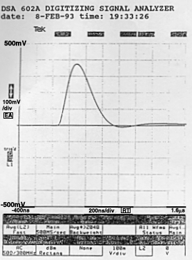
We measured the amplitude of the output signal, peaking time, and gain on six channels of the chip. In order to mimic a minimum ionizing particle, we injected 4fC of charge into the channels; this corresponded to a 0.8mV transition into a 5pF capacitor. The peaking time adjust was set to +2.0V corresponding to the recommended peaking time of approximately 200 nsec on channel 3. The results are shown in Table 1 and are comparable to Fermilab measurements [2]. A sample signal response from channel 1 is shown in Figure 3. There is little variation in response from one channel to the next. The average gain measured over all six channels is 83.9mV/fC.
| CHANNEL# | Vout | PEAK TIME | GAIN |
|---|---|---|---|
| 1 | 340mV | 220ns | 85.00 mv/fC |
| 2 | 350mV | 220ns | 87.50 mv/fC |
| 3 | 340mV | 200ns | 85.00 mv/fC |
| 4 | 320mV | 210ns | 80.00 mv/fC |
| 5 | 340mV | 220ns | 85.00 mv/fC |
| 6 | 325mV | 210ns | 81.25 mv/fC |
The sensitivity of the peak time and gain to the peaking time adjust was measured on a single channel of the chip. The results are shown in Table 2. We found that the gain and peaking time are very sensitive to the peaking time adjust which varies chip to chip.
The dynamic range of the chip was measured by varying the amount of charge injected into a channel. The peaking time adjust is set at 2.0 V. The results are shown in Table 3. The negative polarity signal saturates more quickly than the positive input signal.
| CHANNEL 3 PKA | Vout | PEAK TIME | GAIN |
|---|---|---|---|
| 4.4 | 135mV | 135ns | 33.75 mv/fC |
| 3.5 | 175mV | 150ns | 43.75 mv/fC |
| 2.5 | 255mV | 180ns | 63.75 mv/fC |
| 2.0 | 350mV | 200ns | 87.50 mv/fC |
| 1.5 | 560mV | 310ns | 140.0 mv/fC |
| Qin | Channel 3 Vin | Vout |
|---|---|---|
| 4 fC | 0.8mV | 350mV |
| 8 fC | 1.6mV | 370mV |
| 10 fC | 2.0mV | 420mV |
| 16 fC | 3.0mV | 680mV |
| 20.5 fC | 4.1mV | 840mV |
| 30.0 fC | 5.5mV | saturates |
| -4 fC | -0.8mV | -380mV |
| -8 fC | -1.6mV | -650mV |
| -10 fC | -2.0mV | -830mV |
| -16 fC | -3.0mV | saturates |
| -20.5 fC | -4.1mV | saturates |
| -30.0 fC | -5.5mV | saturates |
Equivalent noise charge (ENC) measurements were also performed. The ENC can be calculated as follows:
where the RMS(noise) is the root mean square of the noise distribution, calculated by the Tektronix DSA and G is the gain measured from the output pulse response. Noise measurements on channel 5 are shown in Table 4 with a variable peaking time adjust (PKA) to yield a peaking time of 200ns. Although reasonable, the noise measurements and resulting slope are larger than what was measured in the tests conducted at Fermilab. Measurements indicate that we still have problems with shielding our detector and electronics properly. We are looking into acquiring proper RF shielding which will further minimize the noise detected in our measurements.
| Capacitance (pF) | PKA (V) | Gain (mv/fC) | RMS noise (mV) | ENC (e) |
|---|---|---|---|---|
| 0 | 2.0 | 82.5 | 17.85 | 1350 |
| 4.7 | 2.0 | 70.0 | 15.77 | 1410 |
| 9.6 | 2.5 | 45.0 | 22.95 | 3180 |
| 15.6 | 2.6 | 38.75 | 22.54 | 3630 |
| 23.7 | 3.1 | 23.75 | 18.04 | 4741 |
| 34.9 | 3.3 | 17.5 | 16.65 | 5938 |