 Send Mail to Jehanne Simon-Gillo
Research Progress on the PHENIX Silicon
Vertex Detector
Jan Boissevain, Tom Carey, Wayne Collier, Barbara Jacak,
Jon Kapustinsky, John Lillberg, Pat McGaughey,
Jehanne Simon-Gillo, Walter Sondheim, John Sullivan,
Hubert van Hecke
Physics Division, MS D456
Los Alamos National Lab
Los Alamos, NM 87545
August 24, 1992
PHENIX-MVD-92-2
1 Introduction
One of the primary goals for the past year has been to learn about and study frontend electronics that could be applicable to the silicon vertex detector. With the aid of Chuck Britton at Oak Ridge National Lab, we have acquired several monolithic eight channel BVXIII Chips and have studied them in detail at Los Alamos National Laboratory. The BVX chip is a CMOS charge sensitive preamplifier-shaper that was designed by Chuck Britton (Oak Ridge National Lab), Ray Yarema and Tom Zimmerman (Fermilab). The chip design is shown in Figure 1 [1]. Each of the eight channels has two shapers and a preamplifier; the channels are at an 84 m pitch. The chip package has 40 contacts which include input and output channels, grounds, drain voltage (Vdd) source voltage, (Vss), bias currents, feedback adjust and peaking time adjust. The drain voltage and source voltage are set to +4.5V and -4.5V, respectively. Each amplifier bias current (pins 7, 8 and 31) comes from a fixed resistor connected to either Vdd or Vss The feedback adjust (pin 12) is connected to an external variable voltage source and discharges the integrating capacitor by offering resistance. The peaking time adjust (pin 28) is also connected to a variable voltage source and can tune the first shaping stage by effecting the feedback resistance. The adjustment of the voltage on this pin will change the gain and the peaking time. [2]
Three BVX chips were tested at Los Alamos National Laboratory in a clean tent with a probe station. Measurements were taken with a Tektronix Digitizing Signal Analyzer (DSA) allowing a direct study of the silicon signals. A Tektronix P6201 x1 FET probe attached to an Alessi MJ1 micromanipulator allows the measurement of high impedance, low capacitance signals and was used to test the chips (Figure 2). Each chip was mounted on and wirebonded to a ceramic hybrid circuit board constructed at LANL. The hybrid board is made of 0.63 mm alumina and the design is shown in Figure 3. Alumina was chosen as the hybrid material because it has the same thermal properties as silicon.
2 Measurements
The DC voltage of each pin in Chip #1 was measured with a microprobe and multimeter. The Vss, measured -4.509 and the Vdd +4.463. Results are shown in Table 1. The values measured were as expected although it is not clearly understood why there is a large variation in DC voltage among the output channels. The input channels are matched to within 1%.
We measured the amplitude of the output signal, peaking time, gain and DC offset on all channels of the chips. In order to mimic a minimum ionizing particle, we injected 4 fC of charge through a probe into each channel; this corresponded to a 0.8 mV transition into a 5 pF capacitor. DC offsets were measured with no input signal. The peaking time adjust and feedback adjust was set to +2.25 Vand 0.600 V so that one can compare these results to previous measurements taken at Fermilab [2]. The results from chips #1 and 2 are in Table 2. The amplitude of the output signal is smaller than measured at Fermilab but the peak time is much shorter. If the peaking time adjust on Chip #2 was set to +1.67, a similar gain to that measured at Fermilab (74 mV/fC) was obtained. The peak time of Chip#1 can be shortened to that of Chip#2 by tuning the peaking time adjust from +2.25 V to +2.72 on Chip#1. For a peaking time adjust of 2.236 V, Chip #3 showed similar results as the first two chips, with an average peak time of 136 ns, an average pulse height of 181 mV and an average gain of 45 mV/fC. Sample signal responses from four different channels on Chip #3 are shown in Figure 4. Although the gain and peaking time is constant within the channels of a chip, there seems to be variation in response from one chip to the next. Similar results were found at Fermilab.
When injecting charge into a single channel, the adjacent channels were checked for crosstalk. Oscillations on the order of +/- 4 mV (2% of the output signal) were measured.
The sensitivity of the peak time and gain to the peaking time adjust was measured on a single channel of each chip. The results are shown in Table 3. We found that the gain and peaking time are very senstive to the peaking time adjust which varies chip to chip.
| Pin Number | Definition | DC Voltage (Volts) |
|---|
| 1 | OUT3 | +0.157 |
| 2 | OUT2 | -0.088 |
| 3 | OUT1 | +0.033 |
| 4 | NO CHARGE | 0 |
| 5 | Vss | -4.397 |
| 6 | NO CHARGE | 0 |
| 7 | BIAS CURRENT | +3.108 |
| 8 | BIAS CURRENT | -4.274 |
| 9 | GROUND | 0 |
| 10 | Vss | -4.395 |
| 11 | Vdd | +4.389 |
| 12 | FEEDBACK ADJUST | -0.644 |
| 13 | GROUND | 0 |
| 14 | NO CHARGE | 0 |
| 15 | Vdd | 4.388 |
| 16 | IN1 | -1.344 |
| 17 | IN2 | -1.351 |
| 18 | IN3 | -1.345 |
| 19 | IN4 | -1.336 |
| 20 | IN5 | -1.338 |
| 21 | IN6 | -1.342 |
| 22 | IN7 | -1.348 |
| 23 | IN8 | -1.341 |
| 24 | NO CHARGE | 0 |
| 25 | Vss | -4.396 |
| 26 | NO CHARGE | 0 |
| 27 | GROUND | 0 |
| 28 | PEAK TIME ADJUST | +2.194 |
| 29 | GROUND | 0 |
| 30 | Vss | -4.396 |
| 31 | BIAS CURRENT | -3.219 |
| 32 | GROUND | 0 |
| 33 | Vdd | +4.404 |
| 34 | NO CHARGE | 0 |
| 35 | Vdd | +4.405 |
| 36 | OUT8 | +0.077 |
| 37 | OUT7 | +0.052 |
| 38 | OUT6 | +0.074 |
| 39 | OUT5 | +0.0075 |
| 40 | OUT4 | +0.127 |
Table 1: DC Voltages of individual 40 pins in Chip #1
Chip #1
Channel# | Vout | PEAK TIME | GAIN | Vout DC | Vin DC |
|---|
| 1 | 205mV | 155ns | 51.25 mv/fC | -32.5mV | -1.34V |
| 2 | 210mV | 150ns | 52.50 mv/fC | -89.5mV | -1.35V |
| 3 | 205mV | 145ns | 51.25 mv/fC | +155.6mV | -1.35V |
| 4 | 210mV | 145ns | 52.50mV/fC | +127.2mV | -1.34V |
| 5 | 210mV | 145ns | 52.50mV/fC | +7.5mV | -1.34V |
| 6 | 210mV | 145ns | 52.50mV/fC | +75.2mV | -1.34V |
| 7 | 207mV | 145ns | 51.75mV/fC | +50.4mV | -1.34V |
| 8 | 207mV | 150ns | 51.75mV/fC | +75.6mV | -1.34V |
| CHIP #2 | | | | | |
|---|
| 1 | 220mV | 140ns | 55.0 mv/fC | +3.4mV | -1.43V |
| 2 | 220mV | 150ns | 55.0mV/fC | -61.3mV | -1.44V |
| 3 | 225mV | 140ns | 56.25mV/fC | +60.9mV | -1.43V |
| 4 | NOT WORKING | | | +46.5mV | -0.67V |
| 5 | 225mV | 140ns | 56.25mV/fC | -117.5mV | -1.44V |
| 6 | 225mV | 140ns | 56.25mV/fC | -8.3mV | -1.45V |
| 7 | 225mV | 140ns | 56.25mV/fC | -13.5mV | -1.44V |
| 8 | 230mV | 140ns | 57.5mV/fC | -75.5mV | -1.43V |
Table 2: Chip Characteristics
Chip #1
PKA | CHANNEL 8
Vout | PEAK TIME | GAIN | COMMENT |
|---|
| 4.4 | 115mV | 110ns | 27.5 mV/fC | overshoot of 15mV |
| 3.5 | 135mV | 125ns | 33.75mV/fC | overshoot of 15mV |
| 2.5 | 187mV | 150ns | 37.5mV/fC | few mV overshoot |
| 2.0 | 240mV | 175ns | 60.0mV/fC | few mV undershoot |
| 1.5 | 340mV | 225ns | 85.0mV/fC | few mV undershoot |
| 1.0 | 680mV | 480ns | 170.0mV/fC | undershoot -25mV |
CHIP #2
PKA | CHANNEL 3
Vout | PEAK TIME | GAIN | COMMENT |
|---|
| 4.4 | 125mV | 105ns | 31.25mV/fC | overshoot of 20mV |
| 3.5 | 155mV | 120ns | 38.75mV/fC | overshoot of 25mV |
| 2.5 | 195mV | 145ns | 48.75mV/fC | few mV overshoot |
| 2.0 | 250mV | 160ns | 62.5mV/fC | few mV undershoot |
| 1.5 | 370mV | 200ns | 92.5mV/fC | few mV undershoot |
| 1.0 | 760mV | 440ns | 190.0mV/fC | |
Table 3: Study of sensitivity of peaking time adjust
The effect of the feedback adjust on the signal amplitude, width, peaking time, and shape was also studied; the results are shown in Table 4. The peaking time adjust was at a value of +2.25 during this test. The feedback adjust did not effect the signal timing or amplitude. The Fermilab group saw that a feedback adjust of -0.600 minimizes the undershoot. We did not see any significant correlation between feedback adjust and signal shape. The peaking time adjust seemed more effective in producing an overshoot or undershoot in the output signal than the feedback adjust. All other tests described in this work were with the feedback adjust set to -0.600 V.
CHIP #2
FEEDBACK ADJUST | CHANNEL 3
Vout | Twidth | PEAK TIME | Voutundershoot |
|---|
| -0.43 | 220mV | 440ns | 140ns | -10mV |
| -0.50 | 220mV | 420ns | 140ns | -10mV |
| -0.60 | 220mV | 420ns | 140ns | -8mV |
| -0.70 | 220mV | 420ns | 140ns | -8mV |
| -0.80 | 220mV | 420ns | 140ns | -8mV |
Table 4: Study of sensitivity of feedback adjust
The dynamic range of the chip was measured by varying the amount of charge injected into a channel. The results for Chip#1 are shown in Table 5. The negative polarity signal saturates more quickly than the positive input signal.
CHIP #1
Qin | CHANNEL 3
Vin | Vout |
|---|
| 4 fC | 0.8mV | 207mV |
| 8 fC | 1.6mV | 410mV |
| 16.5 fC | 3.3mV | 800mV |
| 20.5 fC | 4.1mV | saturates |
| 30.0 fC | 6.0mV | saturates |
| -4 fC | -0.8mV | -205mV |
| -8 fC | -1.6mV | -410mV |
| -16.5 fC | -3.3mV | -590mV |
| -20.5 fC | -4.1mV | saturates |
| -30.0 fC | -6.0mV | saturates |
Table 5: Study of dynamic range
Equivalent noise charge (ENC) measurements were performed on the third BVXIII chip. The ENC can be calculated as follows:
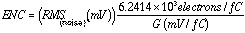 where the RMS(noise)is the root mean square of the noise distribution, calculated by the Tektronix DSA and G is the gain measured from the output pulse response. Noise measurements on channel 2 of Chip#3 are shown in Table 6 with a peaking time adjust of 2.236 V and peak time of 135 ns. The test was repeated on the same channel of Chip#3 with a peaking time value of 1.517 V corresponding to a peak time of 200 ns. The test was also performed in parallel with an HP 3400A true RMS meter to confirm the RMS values given by the Tektronix. The Tektronix and HP yielded similar results with slopes of 38 e/pF and 34 e/pF, respectively. These results are shown in Table 7. In comparison to Table 6, one measures higher noise levels with increasing gain and peak time. These noise slopes are approximately half the value than measured from the tests conducted at Fermilab.
| Capacitance (pF) | Gain (mv/fC) | RMS noise (mV) | END (e) |
|---|
| 0 | 43 | 2.66 | 385 |
| 5.1 | 33 | 2.47 | 460 |
| 9.9 | 27 | 2.76 | 630 |
| 16.7 | 22 | 2.85 | 820 |
| 20.7 | 19 | 2.8 | 915 |
| 32.1 | 15 | 3.07 | 1308 |
Table 6: ENC results Chip #3 Channel #2. Slope=~29e/pF. Test conditions were as follows: Vss = -4.496V, Vdd = +4.500V, Qin = 4.2fC and peaking time adjust = 2.236V.
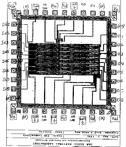
Figure 1: BXVIII Chip Design
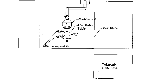
Figure 2: Probe Station utilized for the test presented in this work
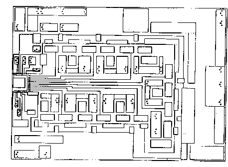
Figure 3: Hybrid Design
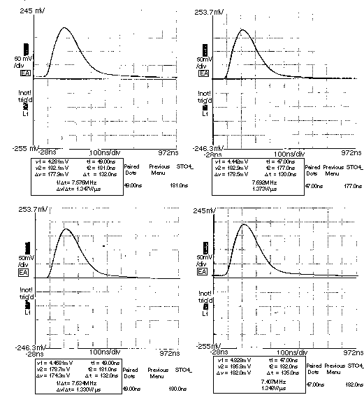
Figure 4: Typical output pulses from Chip#3 upon the injection of 4fC into the chip preamp. There is little variation in response from one channel to the next.
| Cap. | Gain (mV/fC) | noise HP | noise Tek | ENC HP | ENC Tek |
|---|
| 0 pF | 89 | 7.2mV | 6.3mV | 506e | 443e |
| 5.4pF | 67 | 7.3mV | 6.74mV | 679e | 627e |
| 9.9pF | 56 | 7.5mV | 6.8mV | 840e | 761e |
| 16.7pF | 43 | 7.5mV | 6.6mV | 1080e | 950e |
| 20.7pF | 38 | 7.0mV | 5.3mV | 1149e | 870e |
| 32.1pF | 29 | 7.4mV | 7.7mV | 1593e | 1656e |
Table 7: 200 nsec peaking time test on Chip #3, Channel #2. HP slope = ~34 e/pF. Tek slope = ~ 38 e/pF. Test conditions: Peaking Time = 200 nsec, Peaking Time Adjust = 1.517 V, and Qin = 4 fC.
3 Summary
Three BVXIII chips were studied at Los Alamos National Laboratory. Each chip showed consistent results from one channel to the next. One of the eight channels was not functioning on the second chip. There is some variation in response from one chip to the next correlated to the sensitivity of the peaking time adjust. The chips tested at LANL are lower in gain and faster in peaking time than the chips at Fermilab for an equal value of peaking time adjust. Care must be taken when directly comparing the results of our tests to those obtained at Fermilab for it is unclear whether the Fermilab tests had a 10pF capacitor to ground for all of their measurements. There was zero capacitance to ground for the tests performed at Los Alamos.
Other ongoing projects at Los Alamos include designing a laser station to test the response of various recently acquired silicon detectors to minimum ionizing particles and addressing the question of cooling the detector through some preliminary cooling calculations and lab tests with a plenum.
4 Acknowedgements
We would like to thank Jeff Bradley in P14 (LANL) for printing the circuit boards, assembling the hybrids and wirebonding the chips to the hybrids. We would also like to thank Fernando Uribe at Sandia National Laboratory for drilling and cutting the hybrids to the proper size.
5 References and Notes
- Britton, C. Schematic of the N15 BVXIII Chip, Oak Ridge National Laboratory, Instrumentation and Controls Division. May 1, 1991.
- Zimmerman. T. Performance of a New Monolithic Eight Channel Charge Sensitive Preamplifier-Shaper, Fermilab, unpublished, August, 1991.