Equivalent Noise Charge Measurements on
the BVX III Chip
Wayne B. Collier
Princeton University
10 August 1992
Revised by Jehanne Simon-Gillo
Los Alamos National Laboratory,
January, 1993
PHENIX-MVD-92-1
This is a comprehensive report on the work I did during July on the ENC measurements of the BVX III chip designed by Chuck Britton. Jehanne Simon-Gillo and Jan Boissevain have been studying this chip for the RHIC PHENIX collaboration to check out how useful it would be as a front-end amplifier on a silicon strip detector. The report is intended for the use of members of the P2 group here at Los Alamos.
1 Making Equivalent Noise Charge Measurements
The question of ENC measurements came up in Simon-Gillo and Boissevain's work to duplicate the results that Tom Zimmerman got when he studied the BVX III chip at Fermilab in the summer of 1991. Zimmerman's report on his results contained very few details on the exact procedure that he used to make the ENC measurements on the BVX chip, so I relied at the first on a more general, "cookbook" type report that he sent us on how to use the Tektronix DSA 602 digital signal analyzer to make FsNC measurements. Our analyzer is a 602A, and it operates just like the 602, for these measurents, as far as I call tell. (I have not checked the specs on the 602 yet to make sure that it has the same sampling rate.)
In a nutshell, here is the technique I used to make the ENC measurements.
- I learned that it is important to turn on the DSA at least 30 minutes before making the first noise measurements, so that the DSA can through its accuracy enhancement mode calibrations before attempting a noise measurement. Making noise measurements before these internal-temperature compensating adjustments caused me trouble. Consecutive measurements on the same channel gave results 30% or more off from each other. In order for this process to take place automatically, the Accuracy Enhancement box in the modes submenu in the Utility menu must be set to automatic. In this submenu, also select Backweight in the averaging mode box.
- Turn on the FET probe power and the function generator. I generally used a pulse of width 500 nsec and period 500
 sec. The pulse amplitude should be set to about .8 volts to get a 4 fC pulse at the input probe tip.
- Go to the Waveforms menu and ac couple the FET probe input signal. Set its input impedance to 50
 , 20 MHz.
- Still in the Waveforms menu, select Aquire Description. Toggle the averaging on (Hit Average N to `ON'). Select N to be 1024 or greater by selecting the "set N" box and adjusting with the B knobs below the screen.
- Measure the input pulse voltage by touching the FET probe behind the capacitor on the input probe. Make sure that the FET probe is grounded. Once the signal is quiet, the scope can be stopped and paired-dot cursors can be used to measure the pulse height. Calculate Qin, in femtoCoulombs (fC). (For my work, the input pulse passed through a 5 pf 1% capacitor on the probe tip.)
- Reconnect the FET probe, using the probe hook, to the output micropositioner. Input a pulse to the channel you are studying and measure the output signal. After the averaging is complete, stop the scope and again use the paired-dot cursors to measure the pulse height and rise time. Do not use the peak-to-peak measurement mode of the scope, since any signal overshoot will cause it to give an artificially high value. Calculate the gain in mV/fC.
- Lift the input probe from the amplifier input. Disconnect the output cable from the function generator, or turn the function generator off. Failing to do this could cause a false signal to be transmitted to the amplifier input, unless the micropositoner tip is more than about 3 inches away from the amp input. I found it easiest to just disconnect the cable after lifting the probe tip off the amp input.
- Prepare to take the RMS noise measurements now by selecting the measurements menu. Select the measurements box. Select
 RMS. In this submenu, under Data Interval, select Whole Zone measurement. This is an important point, since the signal is random and therefore measuring by periods does not give consistent results. After selecting Whole Zone, you may want to remove the red annotation bars by pressing the tiny "Rem Anno" box that will appear just below the graticule.
- Set the FET probe positioner on the desired output strip. Set the volts/div vertical scale as low as possible, with the signal still remaining smaller than the screen height. This was usually 5 mV/div for my measurements. Note that the scope resolution is 8 bits, which Jan and I interpret to mean that the vertical scale includes 256 data points. For 5 mV/div, this means that each data point has a "width" of 0.195 mV. I considered this to be the intrinsic error in the RMS measurement, although one may argue that the error should be +- half this value.
- Cover the box to eliminate as much external noise as possible. Make sure that you return the probe to the output strip if putting the lid on knocked it off.
- Select the Statistics page in the main Measurements menu. Select the Statistics box. Select Live Waveform Stats and turn stats ON. Select "Set Statistics N". Use the knobs below to set N=3000 or more. Press reset to start a new measurement. The "Sample #" box should start counting up. If it does not, turn the FET waveform off and on with the button right by the input to the scope. Then return to the Statistics box and reset for a new measurement. Each measurement takes between ten and twelve minutes.
Note:
When the scope performs summation-type averaging on a waveform, it calculates the average over the desired number of samples, then outputs a single "answer" waveform. It also outputs an ARMS value in the Measurments menu. This value is not accurate. Apparently, the scope does not actually calculate this value for all of the sampled and summed waveforms. Only the Statisticsmode RMS mean value gives consistent, reasonable results that correspond reasonably to the magnitude of the noise signal.
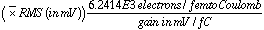
12. Calculate the Equivalent Noise Charge thus:
13. Begin the next measurement by attaching a new capacitor between the input and ground. Input the pulse on the input side of the capacitor and proceed as before from step # 6. (The RMS will remain in Whole Zone mode, so it does not need to be changed back.)
Some preliminary notes on noise:
From the beginning of the chip study, noise was a problem. For a while, we thought that the chip was oscillating internally at about 35 kHz, since this periodic noise kept showing up. Then Chuck Britton, of ORNL, pointed out that color monitors often produce noise at this frequency. I confirmed that this noise was coming from the DSA screen by attaching a long piece of wire to the FET probe which was providing our input to the scope, and moving this antenna around. The 35 kHz signal was by far the largest when the wire was in front of the DSA screen. Moving the FET probe cable and the function generator output cable away from the DSA screen reduced this oscillation considerably.
To improve the Caliphs shielding even more, I covered the holes in the box cover with copper plates that can fold back for access to the micromanipulators and for viewing the chip through the microscope. This shielding pretty well eliminated the noise produced by the lights in the clean tent. Then I performed a Fast Fourier transform on the chip's output, with the chip powered up, but without an input signal. To do the FFT, display the waveform you are studying in Continuous mode, but display the FFT plot in Averaging mode.
The FFT showed that external noise was still getting into the box, and being picked up by the FET probe from the chip outputs. Noise signals came in at about 8 Hz, 25 Hz, 230 Hz, 2 kHz, 7 kHz, 18 kHz, 32 kHz, 67 kHz, 431 kHz, 1 MHz, 1.4 Mhz, 2.06 MHz, 3.6 MHz, and 11.5 MHz. Then there was a broad space of quiet, followed by a wide expanse of strong signals beginning at 1 GHz and continuing beyond 30 GHz in increments of .5 GHZ. Jan pointed out that although these signals look something like radar or communications signals, they are probably just nonsense, since the scope only samples at 2Gs/sec.
So noise still gets through, even with the copper box enclosure. The most interesting thing about this FFT measurement, to me, was that the hybrid seems to be responsible for picking up almost all of this noise. The FFT spectrum for a hybrid channel which was not connected to the chip turned out to be very similar to the other channels which were connected to the chip. This made me decide to make some later ENC measurements with the chip output disconnected from the hybrid to get a more direct measurement of the chip's internal noise.
2 Chronology
Before my work on the ENC measurements, I spent several days learning how to reproduce Simon and Bossevain's earlier results on the chips, besides trying to understand the general noise problems of the chip. My first step was to repeat the gain and risetime results for chip #1. This test was flawed because I did not measure the input pulse height to make sure of the gain. For this test peak time adjust was set at 2.25 Volts, and feedback adjust was at .6 volts. These measurements were taken by stopping a waveform that was in Continous mode, because I had not learned about Averaging mode yet. At the time, I thought that the measurements probably had an error of about 6 mV in the height and about 2 nsec in the rise time. I now know that this assumption was flawed for at least two reasons. First of all, I used the line cursors instead of the paired-dot cursors for these measurements. Since the paired-dot cursors move from data point to data point right along the waveform, they are more accurate. Secondly, I now accept that it is difficult to be sure to within 7 nsec of exactly where a waveform begins and ends its rise.
| Channel |  Vout Vout | Rise Time |
|---|
| 1 | 208 mV | 150 nsec |
| 2 | 218 mV | 150 nsec |
| 3 | 206 mV | 150 nsec |
| 4 | 210 mV | 152 nsec |
| 5 | 214 mV | 148 nsec |
| 6 | 214 mV | 148 nsec |
| 7 | 214 mV | 148 nsec |
| 8 | 212 mV | 148 nsec |
Table 1: First Test on Chip # 1
For the next several days, I learned how to use Microsoft Excel on a Macintosh computer to print out the waveforms saved by the DSA 602A to diskette. I finally perfected the procedure. Step by step, it follows here. Just recently, however, I learned that the DSA is capable of making paper printouts of its waveforms through a direct connection to a laserprinter, and I have used this simpler technique ever since. Besides its ease, the hardcopy method is interesting because the copies can include a picture of the entire screen, with the measurement parameters still showing. On the other hand, the Excel method produces larger, more elegant graphs, without the graticule grid that shows up in the hardcopy method.
To make copies using Excel;
- Initialize a 3.5" diskette to function in DOS. I used the Apple File Exchange program to do this, but the DSA can do it, too, using its format command in the Disk Ops submenu of the third page of the Utility menu.
- Stop the waveform with the Run/Armed /Stop button
- Go to the third page of the Utility menu. Select File Ops.
- Select File Type and toggle it to "Waveform".
- Select File Data Type and toggle it to "Worksheet.WF1"
- Select the Store/Recall Menu
- Select "Store Waveform". Select the tiny "DISK" box
- Select "Set Next STO Index". Set this number with the knobs
- Select the box that contains the name or the waveform you are saving.
- Now the waveform is saved to disk. Open up Apple File Exchange on a Mac and insert the disk.
- Transfer the worksheet that contains your waveform data to the hard drive.
- Exit AFE and enter Excel.
- Go to the "Open" command. Select "Text" in the box that comes up.
- Select "Comma" as the column delineator. Select "ok".
- Open the waveform.
- Select the entire worksheet by clicking in the little empty box in the top left corner.
- Press F11. Select "X-values in X-Y chart" in the menu that pops up.
- When the graph shows up, go to the gallery menu and select the line graph option. Choose the simplest type (no markers).
- Click on the x-axis. Select "scale" and in that box choose the options of displaying a tick mark and a tick label for every 50 data points.
- In the pattern menu of the x-axis window, place the minor tick marks outside the axis. Don't display the major tick marks.
- Exit the x-axis window by pressing "ok" and click on the y-axis. In the patterns menu, let the major tick marks cross the y-axis, and put the minor tick marks outside the axis.
- In the scale menu, choose to have the x-axis cross at the minimum y value displayed.
- Exit by pressing "ok". The graph should look finished. Select "Set preferences" in the Gallery menu to set this as your default graph design. Next time you can skip steps 18-21 by selecting "Preferences" after the graph is first produced.
- Now you're ready to print.
Obviously, this is a terribly tedious way of getting a graph. The hardcopy method is much easier. I'll explain it here.
For a hardcopy on an HP laserprinter (several others are possible):
- Set up the scope by selecting the Utility menu. Go to the second page. Select the Hardcopy box.
- Select "Printer" and toggle to "Alt. Ink Jet".
- Select Direction Horizontal.
- Select Screen Format HiRes.
- Set Security Option off, unless you want all the data on the screen to be hidden. Security Option "on" shows just the waveform and the grid.
- Return to your waveform. Make sure the printer is on and connected. To make a hardcopy, just press the hardcopy button on the scope face.
- Perhaps the most useful way to matte a hardcopy is to take the picture while the screen is displaying the cursors and their measurements. Of course, you can use any ether configuration of the screen that you like.
I spent the next few days looking at the 35 kHz ringing, which, we have now concluded came from the scope screen all along. This ringing has not been
much of a problem since I moved the input and output cables farther from the scope.
On July 9, I called Chuck Britton to ask his ideas about the ringing. He said not to worry about it, and asked me to send some sort of picture to indicate to him that I was on the right track. I sent him a signal including positive and negative output pulses, but without lots of useful information that I later learned he would need, like the gain, etc.
Also on the 9th I learned about Averaging Mode. This was to change my life forever.
On July 10, I began to look more closely at chip #2, with the intention of reproducing Bossevain and Simon-Gillo's results. For this set of measurements I forgot that the FET probe input was ac coupled, so my measurements of the dc offset were nonsense, of course. Here are my other results, though. I used the paired-dot cursors for these measurements. Vss= -4.497; Vdd = +4.497. Volts/div= 50 mV. Sweep time= 100 nsec. Input pulse = 4.4 fC. Peaking Time Adjust Voltage= 1.625 V.
| Channel # | Vout | Peaking TIme | Gain | Saved as |
|---|
| 1 | 159 mV | 170 nsec | 36.1 mV/fC | STO 30.WF1 |
| 2 | 157 mV | 172 nsec | 35.7 mV/fC | STO 29.WF1 |
| 3 | 158 mV | 171 nsec | 35.9 mV/fC | STO 28.WF1 |
| 4 | Not Working | | | |
| 5 | 156 mV | 163 nsec | 35.5 mV/fC | STO 27.WF1 |
| 6 | 156 mV | 169 nsec | 35.5 mV/fC | STO 26.WF1 |
| 7 | 156 mV | 175 nsec | 35.5 mV/fC | STO 25.WF1 |
| 8 | 157 mV | 170 nsec | 35.7 mV/fC | STO 24.WF1 |
Table 2: July 10 Channel-by-Channel test of Chip #2
Also on July 10th, I tested a single channel (#5) through many peaking times. The results follow here. For this set of measurements, Vss= -4.497, Vdd = +4.497, sweep time = 1sec, Input pulse = 4.4 fC.
I sent a fax containing these results to Chuck Britton on June 10. Notice that the overshoot reached 13% of the total pulse height at 4.4 Volts. As the height of the overshoot increased, it also began to indent on the side toward the pulse, making it look like a tiny reflection of the original pulse.
Next I tested chip #3 for its overall performance. When I first tested its third channel, I thought it was not working, so I did not have it wirebonded when the other channels were. I later discovered that it was working, so l made measurements on that channel directly to the chip's input and output. These results are included in the graph, but what you don't see is that this output signal (channel #3) was shaped a little differently than the others. The peak had a slight indention on its rising side near the top.
For this set of measurements, the parameters were: (Notice that this time I took more care to record the scope setup.) FET input 50, 20 MHz, backweight-type Averaging with 128 samples, peaking time adjust voltage fixed at 2.236 V (no potentiometer on this hybrid), sweep time=100 nsec, Volts/div=50 mV, Input pulse=4.0 fC, measurement with paired dots.
| P.T. Adj. | tpeak | Vout | Gain | Step ht. | Step wdth | Stored as |
|---|
| 1.00 V | 400 ns | 382 mV | 86.8 mV/fC | | | STO 31.WF1 |
| 1.25 V | 258 ns | 238 mV | 54.1mV/fC | -5.5 mV | | STO 32.WF1 |
| 1.50 V | 191 ns | 176 mV | 40.0 mV/fC | -2.4 mV | | STO 33.WF1 |
| 2.00 V | 145 ns | 123 mV | 28.0 mV/fC | 3.5 mV | 250 nsec | STO 34.WF1 |
| 2.50 V | 132 ns | 97.7 mV | 22.2 mV/fC | 6.5 mV | 350 nsec | STO 35 WF1 |
| 3.00 V | 119 ns | 81.7 mV | 18.6 mV/fC | 7.7 mV | 350 nsec | STO 36.WF1 |
| 3.50 V | 108 ns | 71.6 mV | 16.3 mV/fC | 8.4 mV | 350 nsec | STO 37.WF1 |
| 4.00 V | 98 ns | 65 mV | 15 mV/fC | 8.5 mV | 275 nsec | STO 38.WF1 |
| 4.40 V | 88 ns | 60 mV | 14 mV/fC | 8 mV | 220 nsec | STO 39.WF1 |
Table 3: Peaking Time dependence of Gain on Chip #2, channel #5
| Channel # | Peaking Time | Vout | Gain | Stored as |
| 1 | 135 nsec | 177 mV | 44 mV/fC | STO 47.WF1 |
| 2 | 135 nsec | 179 mV | 45 mV/fC | STO 46.WF1 |
| 3 | 140 nsec | 196 mV | 49 mV/fC | STO 45.WF1 |
| 4 | 136 nsec | 180 mV | 45 mV/fC | STO 44.WF1 |
| 5 | 135 nsec | 178 mV | 45 mV/fC | STO 43.WF1 |
| 6 | 136 nsec | 176 mV | 44 mV/fC | STO 42.WF1 |
| 7 | 135 nsec | 180 mV | 45 mV/fC | STO 41.WF1 |
| 8 | 136 nsec | 183 mV | 46 mV/fC | STO 40.WF1 |
Table 4: Chip #3, Channel by Channel
Next, I was concerned that perhaps the extra leads that I attached to the outputs of chip #3 might add a significant stray capacitance to the outputs, thus cutting down the gain. This concern was boosted by the higher gain on channel #3, which was not connected to the hybrid or the output leads. I performed a simple test to see if this was the case, but now I think that it was flawed. Here's why: In previous test, I input the signals on a capton strip which was wirebonded to the input ports of the amplifier. For this test, I input the signal at the end of the extra leads. The idea was that if the stray capacitance was affecting the signal, the effect would be exaggerated if the pulse were placed at the end of the extra input lead. Now, though, I think that it is more likely that the effect of the extra leads was just the same, whether the signal was input at their beginning or end. So I am not certain that I know exactly what the effect of the extra leads is. However, if I assume that they cause the difference in gain observed in channel #3, then the effect is on the order of an 8% reduction in gain.
At this point, on about July 13, I began studying how to do the ENC measurements. At first I tried taking the rms mean by using summation averaging of the signal and then reading the rms mean value given in the meausurements menu. This was nonsense, apparently. I spent about a week trying to figure this out. During one of my tests, I somehow ruined channel #4 of chip #3.
My first reasonable measurements come on a test of Chip #3, Channel #5. This was a preliminary test, and I had not refined the measurement technique
yet. Still, I got a slope of 19 e/pf, which indicated to me that I was getting somewhere near the right method. Sweep time for these measurements was 100 nsec.
After some experiments with the effects of temperature changes on the calculated rms value, I decided that the enhanced accuracy mode of the scope does improve the consistency of the values given by the statistics algorithrns. I used enhanced accuracy from this point on out.
Also this week I built the heating test plenum and started some preliminary tests on it.
I measured the inherent noise of the FET probe and scope to have a value of about 200 volts. This introduces an error in the ENC measurements ranging from about 15 to 50e, for the highest to the lowest measured gains, respectively.
The next set of ENC measurements was on Chip #3, channel #6. I used the method of the beginning of the paper for these measurements, but with one mistake. I used the measurement mode of the scope to get the output pulse height, and at higher capacitances this resulted in an inflated value for the gain, because the measurement mode included the undershoot caused at these higher capacitances as part of the pulse height. So as a result, the slope is unnaturally low. The results follow. Parameters: Whole Zone measurements. Statistics N = 3000. Sweep Time = 100 nsec. Peaking Time adjust = 2.236 V, peaking time = 136 nsec Qin = 4.3 fC. See Table 5.
I repeated this test on Channel #1. Whole Zone measurements. Statistics N=3000. Sweep time = 100 nsec/div. Qin = 4.3 fC. See Table 6.
Next, l realized my error about the measurements of the gain, so I decided to repeat the measurements on channel #6. At the same time, I decided to disconnect the output from the hybrid, because I suspected that the hybrid was acting like an antenna for noise, artificially pushing the value higher. See Table 7.
| Capacitance (pF) | Gain (mV/fC) | RMS noise (mV) | ENC (e) |
|---|
| 0 | 41 | 2.33 | 354 |
| 4.8 | 32 | 2.59 | 508 |
| 9.5 | 27 | 2.77 | 654 |
| 14.7 | 22 | 2.76 | 790 |
| 21.5 | 18 | 2.67 | 943 |
| 35.7 | 13 | 2.71 | 1295 |
Table 5: ENC results for Chip #3, Channel #6. Slope = approx 26 e/pF.
| Capacitance (pF) | Gain (mV/fC) | RMS noise (mV) | ENC (e) |
|---|
| 0 | 47 | 2.65 | 355 |
| 4.7 | 38 | 2.66 | 442 |
| 9.6 | 31 | 2.78 | 560 |
| 15.6 | 25 | 2.81 | 707 |
| 23.7 | 20 | 2.92 | 920 |
| 34.9 | 16 | 2.94 | 1151 |
Table 6: ENC resutls for Chip #3, Channel #1
| Capacitance (pF) | Gain (mV/fC) | RMS noise (mV) | ENC (e) |
|---|
| 0 | 38 | 2.57 | 420 |
| 4.8 | 30 | 2.6 | 545 |
| 9.5 | 25 | 2.65 | 650 |
| 14.7 | 20 | 2.68 | 855 |
| 21.5 | 17 | 2.73 | 1000 |
| 35.7 | 16 | 2.8 | 1110 |
Table 7: Corrected ENC results for Channel #6. Slope = approx. 20 e/pF
On July 28, I continued the tests, this time on Chip #3, Channel #2 . Vss = -4.496 V. Vdd= + 4.500 V. Sweep time = 100 nsec/div. Pulse width = 1 sec, pulse frequency = 450 sec (2.22 kHz). Qin = 4.2 fC. Whole Zone Measurements, N = 3000. See Table 8.
Next, I disconnected the output of Channel #2 from the hybrid, and rechecked the noise levels. The noise slope was lower.
This Channel #2 is the main channel that I used for later measurements.
Responding to a request from Jehanne, I repeated some of the earlier tests on Chip #2 to see if I got the same results using averaging mode as she got using continuous mode. This was to make sure that the results in the earlier report were in fact accurate. The two sets of results did agree to within the normal error margins for measurements on this scope. However, it will probably be necessary to repeat all of the measurements in the earlier report, if we want to compare our results with Tom Zimmerman's, because it looks now like Tom hung a 10 pF capacitor to ground for all of the measurements that Simon-Gillo and Boissevain were comparing theirs with. Boissevain and Simon-Gillo used O pF capacitance to ground for these measurements.
For the next week I did more heating tests with Jan while waiting for repairs to the hybrids.
| Capacitance (pF) | Gain (mV/fC) | RMS noise (mV) | ENC (e) |
|---|
| 0 | 43 | 2.66 | 385 |
| 5.1 | 33 | 2.47 | 460 |
| 9.9 | 27 | 2.76 | 630 |
| 16.7 | 22 | 2.85 | 820 |
| 20.7 | 19 | 2.8 | 915 |
| 32.1 | 15 | 3.07 | 1308 |
Table 8: ENC results Chip #3 Channel #2. Slope = approx 29 e/pF.
| Capacitance (pF) | Gain (mV/fC) | RMS noise (mV) | ENC (e) |
|---|
| 0 | 43 | 2.35 | 340 |
| 5.1 | 33 | 2.40 | 455 |
| 9.9 | 27 | 2.46 | 565 |
| 16.7 | 22 | 2.50 | 725 |
| 20.7 | 19 | 2.51 | 845 |
| 32.1 | 14.7 | 2.54 | 1077 |
Table 9: ENC results on Chip #3 Channel #2, with output disconnected from hybrid. Slope = approx. 23 e/pF
On August 6th, I had a conversation with Chuck Britton in which he questioned my results and asked me to use an HP 3400A true RMS meter to confirm the RMS values given by the Tektronix. I borrowed one from Song Koo Hahn's section over in the SST division. He also asked me to increase my sweeping time to 5 sec/div, and to also look at the peak-to-peak value of the output's white noise. He pointed out that this amplitude is usually 6 , so that division by six gives a rough estimate of the RMS noise value. Armed with these two new benchmarks, I prepared for a new set of measurements. Chuck also wanted me to take this set of measurements at a peaking time of 200 nsec, because he has decided to use this peaking time as a benchmark of comparison between tests on different chips in different places. As I was preparing for the test, however, I noticed that my entire output noise signal was now superimposed on a 20 mV peak to peak, 60 Hz signal. In fact, the entire ground plane was oscillating at this frequency-even the ground pin of the clean power. I was unable to find the source of this noise, and decided to take measurements, anyway, since Chuck was looking for me to get a slope 2.5 times higher than I had acheived so far, and I guessed that a constant underlying noise signal in the ground plane would not have that great an effect on the noise response slope. Since by this time I had learned how to make hardcopies of the scope screen output, I included these pictures in my lab book. They begin on page 74.
Chip #3, Channel #2. Trigger: pulse from HP 8082A (like always), width = 500 nsec, period = .1 msec (10 kHz). Peaking Time = 200 nsec. Peaking time Adjust = 1.517 V. Qin = 4 fC.
, so that division by six gives a rough estimate of the RMS noise value. Armed with these two new benchmarks, I prepared for a new set of measurements. Chuck also wanted me to take this set of measurements at a peaking time of 200 nsec, because he has decided to use this peaking time as a benchmark of comparison between tests on different chips in different places. As I was preparing for the test, however, I noticed that my entire output noise signal was now superimposed on a 20 mV peak to peak, 60 Hz signal. In fact, the entire ground plane was oscillating at this frequency-even the ground pin of the clean power. I was unable to find the source of this noise, and decided to take measurements, anyway, since Chuck was looking for me to get a slope 2.5 times higher than I had acheived so far, and I guessed that a constant underlying noise signal in the ground plane would not have that great an effect on the noise response slope. Since by this time I had learned how to make hardcopies of the scope screen output, I included these pictures in my lab book. They begin on page 74.
Chip #3, Channel #2. Trigger: pulse from HP 8082A (like always), width = 500 nsec, period = .1 msec (10 kHz). Peaking Time = 200 nsec. Peaking time Adjust = 1.517 V. Qin = 4 fC.
| Cap. | Gain (mV/fC) | noise HP | noise Tek | ENC HP | ENC Tek |
|---|
| 0 pF | 89 | 7.2 mV | 6.3 mV | 506 e | 443 e |
| 5.4 pF | 67 | 7.3 mV | 6.74 mV | 679 e | 627 e |
| 9.9 pF | 56 | 7.5 mV | 6.8 mV | 840 e | 761 e |
| 16.7 pF | 43 | 7.5 mV | 6.6 mV | 1080 e | 950 e |
| 20.7 pF | 38 | 7.0 mV | 5.3 mV | 1149 e | 870 e |
| 32.1 pF | 29 | 7.4 mV | 7.7 mV | 1593 e | 1656 e |
Table 10: 200 nsec peaking time test on Chip #3, Channel #2. HP slope = approx 24 e/pF. Tek slope = approx 38 e/pF.
After receiving these results from me by e-mail, Chuck Britton asked me to send one of the chips from this same run (NlAU) to Ray Yarema at Fermilab. I did this on August 10.