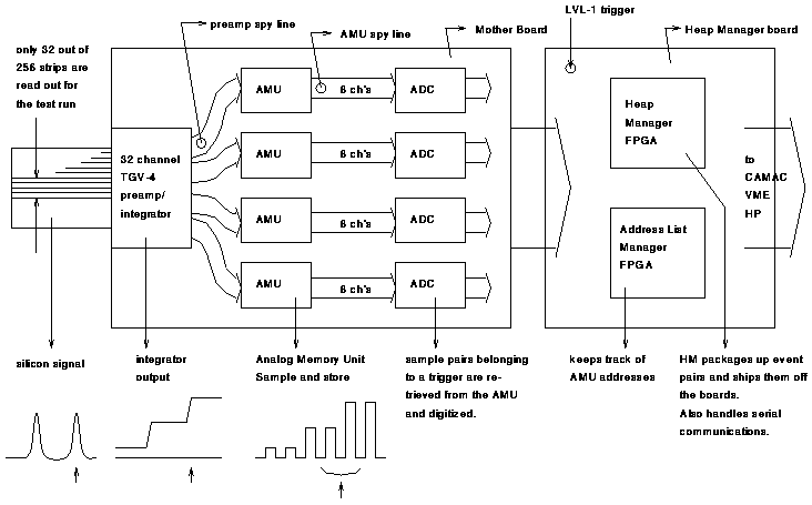
BEAMTEST PROTOTYPE FEE BOARDS
Below you can see a schematic drawing of the beamtest
prototype FEE boards.
From left to right you can see:
- The silicon strip detector. Only 32 out of 256 200-micron-pitch channels
were wired up for the test. Small charge pulses are generated when
particles traverse a channel. The silicon is connected by a 20 cm kapton
cable to:
- the TGV-4 preamp/integrator. This unit is an open integrator, such that the
output jumps each time a signal is generated by the silicon. The
integrator is reset every 1K (2K,4K,8K) beam clock cycles. The output
voltage for every channel is sampled each beam clock and samples are
stored in the:
- the AMU, or analog memory units. When a LVL-1 trigger is received on the
Heap Manager board on the right, the HM Field-Programmable Gate Array,
who is the chief of this little domain, instructs the Address List
Manager FPGA to calculate the addresses of the AMU cells where the
appropriate voltage sample pairs are held. The AMUs then deliver the
samples to the ADCs, and the HM collects all digitized information, and
packages it up into two events: one corresponding to the instant just
before the trigger event occurred, and the second event corresponding to a
snapshot one beam cycle later.