![[multiplexed serial readout...]](../../gifs/arrow.marble.left.gif)
|
![[introduction]](../../gifs/arrow.marble.up.gif)
|
![[PECL clock test]](../../gifs/arrow.marble.right.gif)
Previous page
| Up to the index
| Next page
| |
![[multiplexed serial readout...]](../../gifs/arrow.marble.left.gif)
|
![[introduction]](../../gifs/arrow.marble.up.gif)
|
![[PECL clock test]](../../gifs/arrow.marble.right.gif)
Previous page
| Up to the index
| Next page
| |
A minor fault in the previous setup
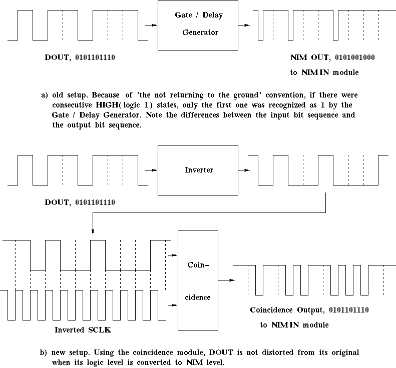
We have completely solved the problem of MAX186 ADC response. Conclusively, now MAX186 ADC shows a definite linear response. At first, we tried to make the conversion clock faster using the internal clock mode. In the internal clock mode, MAX186 ADC generates its own conversion clock so that the conversion time can not exceed a certain limit if the external clock is too slow. By the internal clock mode test, we became to know that the clock speed was really not the reason for the non-linear ADC response, because we obtained the same non-linear ADC response from that test. The reason was a minor fault in the setup to read out ADCs. It is explained in Fig 1.

Fig 1. Change in the setup
Suppose that data out from ADC is consist of 10 bits and its bit
sequence is 0101101110. In the case of the old setup, the logic
level of this data
out signal is converted to NIM level for further process
by going through a Gate/Delay generator. But the bit sequence of
the data out
from the Gate/Delay generator is different from the
original bit sequence because MAX186
ADC follows 'the not returning to the ground' convention for
the data output signal as shown in Fig 1. So we replaced the
Gate/Delay generator with a Coincidence module( a kind of logic
AND gate ). Inputs to the Coincidence module were DOUT and SCLK
which were inverted by a inverter. Now the logic level converting
process does not affect the bit sequence of the data out any longer.

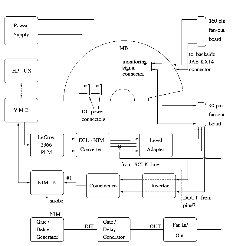
Fig 2. Block diagram of the new setup
The new ADC response
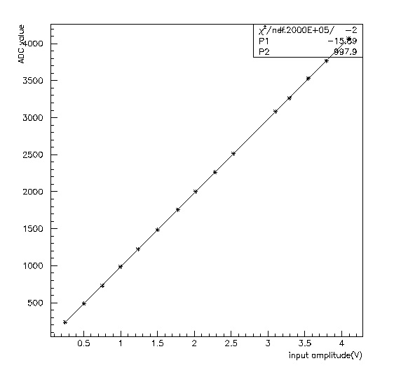
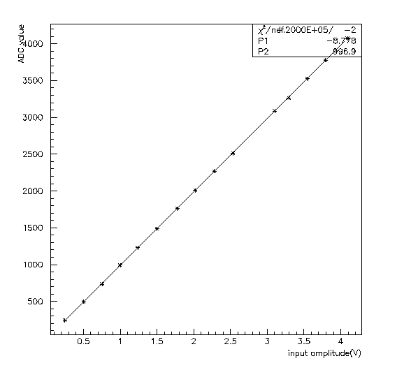
After we modified the setup, we took the ADC output data for inputs with an interval of about 0.25V. Both clock mode were tested. The resulting ADC response was linear for each clock mode. Though the ADC output value from the internal clock mode operation was little bit greater than the ADC output value from the external clock mode operation for the same input, there was no significant difference between the results from both clock mode operations. At large, the coversion gain of the ADC was 997ch/V which is very close to the ideal conversion gain 1000ch/V.

Fig 3. The new ADC response in the external clock mode.

Fig 4. The new ADC response in the internal clock mode.
