MVD DCIM test procedure


This document is based on notes I made 15-Oct-1999 when Miljko Bobrek explained the Data Collection Interface Module (DCIM) test procedure to me. This first version of the document is a transcription of notes I wrote in the logbook while talking to Miljko. Therefore it is not always in the most logical order.

The program to do the test is called chaintest\dcim_ctrl\IM_tester.vi. To use the program, the "VME-chzy" card (made by SangYeol Kim) and the Timing and Control Interface module (TCIM) must be removed from the interface module crate. Test card 3/4 (TC34) must be in the interface module crate.
To start the program, click on the arrow button in the top left corner of the program's panel.

  • connect the ribbon cable from the DCIM input to connector J3 (3rd from top) on TC34.
  • click MiniDAQ Reset
  • program DCIM -- used file chaintest\dcim_ctrl\dcim0928.hex.
    open
    download (it takes approximately forever)
    when it's done, hit exit
  • check DONE bits. Need to set module address in this panel (e.g. 3E on the prototype board we have). The module address is set by jumpers on the DCIM board. I think that the address is 3F if there are no jumpers connected. Hit SET. There should be 5 LEDs on. Then exit.
  • Glink done bits are similar, but you need to test the DONE bits (previous step) first because that's where it gets the module address. Hit check Glinks. You can also reset the Glinks. This sometimes works if they are not locked. The numbering of the Glinks is "correct" -- it goes from 1 ... 6 from top to bottom of the module.
  • set corr/raw mode bit
  • for MUX mode (2 channels output from one DCIM channel) use DCIM/DCM 2:1.
  • DCIM reset does not do anything (anymore). This is done with mode bit 5. Used if there is some garbage in the FIFOs -- which will keep screwing things up (since program reads correct number of bits) for every event until it is reset.
  • miniDAQ reset if miniDAQ fifo is not empty.
  • send packets: Can set BC, AMU1, AMU2 in header of sample packets. Can select count or random -- count only goes to 8 bits, so it does not check all bits. Can turn off one or more of the 6 channels. Then hit "send packets". This sets up data to be sent to the DCIM fifos, but it will not be sent out until you hit ENDDAT0 or 1. Then packets should go to the miniDAQ and you should see the miniDAQ fifo go to "DATA".
  • The hit "get packets".
  • FIFO 1,3,5 and FIFO 2,4,6 are just indicators of how many packets are in the DCM fifos. If you hit ENDDAT0 and 1 with no valid data in the FIFOs, it will still send a packet, but with no valid data.
  • Continuous run -- goes through the sequence send packets --> ENDDAT0 --> ENDDAT1 --> Get packets --> Display --> repeat ...


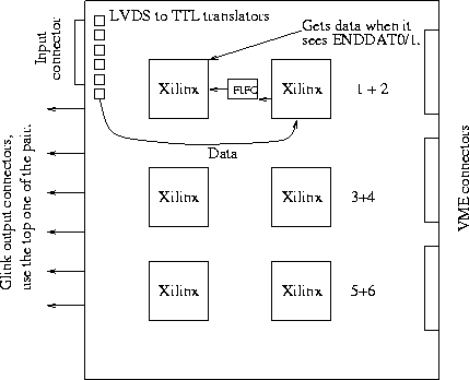
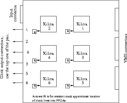
    We should have the following schematics:

  • 6 sheets of Glink schematics (identical)
  • 3 sheets (identical) for pairs of channels
  • 1 schematic for the "VME" section -- near the connectors and power supplies.
  • 1 top level schematic which shows the blocks from the schematics above.
  • There are 7 input 6.5V lines


    To start test, plug the board in and make sure the 2 red lights on the front come on. Check that every regulator has +5V:

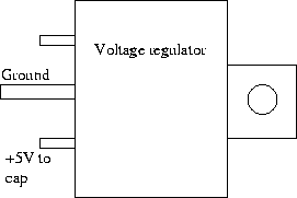
    If they are not all OK, check the 6.5V input. If there is no 5V, there is either a short in the 5V line(s) or no 6.5V input.

    Oscillator section: take the beam clock from TC34. The 4X clock is generated from the beam clock. Jumpers are undes to set the output frequency. The approximate clock location is shown in the sketch (above) of the DCIM board with more details in the following sketch:.

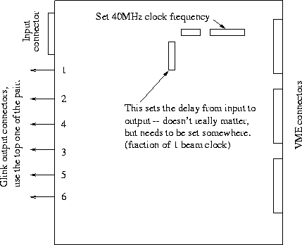
    The clock needs to be tested at the oscillator (1X --> 4X). Also check the beam clock at the input to the FPGAs:


    Try to program the FPGAs

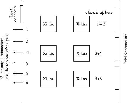
    The address of each board must be set using jumpers (J11). The address must be different for each board. The jumper is a set of 6 pairs of pins near the back (VME connectors) of the board. It seems that no connection corresponds to "1" and the top pair of pins corresponds to the lowest order bit. The address is used to read back done bits. You need to go through all 6 values of the done mux (DMUX in labview) because there is a single done output line. The done bits correspond to the 6 FPGA numbers (see figure above), not to the MCM number.
    DMUX value in program FPGA number, counting as in sketch above
    1 6
    2 5
    3 2
    4 1
    5 4
    6 3

    Check Glinxs with Glink MUXs. The translation of MUX value to Glink value is shown in the table below. The same MUXs are used for the Glink reset command.
    GMUX value in program Glinx number, counting top to bottom
    1 5
    2 6
    3 1
    4 2
    5 3
    6 4

    When the FPGAs are programmed correctly, the 6 green lights on the fromt panel should come on, the counting is 1,2,3,4,5,6 (reeading left to right and top to bottom -- as you would read page of text). Again, these are FPGA numbers, not MCM numbers. These lights are the same as the done bits you read back.

    The FPGA download is in parallel to all FPGAs. Only the done bits are multiplexed. One the FPGAs are programmed, they should send the 20 MHz clock to the Glinks. The STROBE inputs should get the 20MHz clock from the FPGAs. DV0 and DV1 should be set for 20 MHz mode. Miljko thought it was DV0=high, DV1=low, but said it might be vice-versa. These signals come from the FPGAs. That's about all there is to check on the Glinks.

    Jumper JMP1 needs to be set with M20SEL to +5V (jumper pins 3-4) --> 16 bit mode. Therefore it seems that it is really M20SEL-bar.

    One problem Miljko saw was a stuck bit -- in this case the problem was the Glink transmitter chip (parallel to serial converter).

    Send packets and look at them to make sure they are OK.


    Potential problems

  • LVDS --> TTL translators. The data lines are dataA, dataB, and clock. There are six resistors on these lines intoi each FPGA (2,4,6). The start of a data packet is clock line high while dataA goes up and down 4 times. If this is seen, it means the FPGA got the beginning of a data packet, so there should be some output packet.
  • When you send a packet, you should see DONE pulses at J4 and J5 (big round holes near FPGA 2,4,6). If there is no done pulse, either there is no input, no FPGA program, or the FPGA is bad. If there is a done pulse, then the fifo should have data. Miljko says the fifos are reliable. If they do not work, it is probably the soldering. When the fifo gets data the empty flag goes high (empty=0V, at least 1 bit of data in fifo=+5V).
  • When FPGAs 1,3,5 get ENDDAT0/1, they empty the fifos. These FPGAs also send CAV and DAV to Glink chip.
  • 262 words come out of FPGAs 2, 4, 6 (correlator mode) and into the FIFOs. The FIFOs will hold 262*7 words.
  • FPGAs 1, 3, 5 generate DCIM 273 word packets. If FPGAs 1, 3, 5 get ENDDAT, then they will send out a packet -- no matter what. If they do not, check
    1) 40 MHz clock
    2) ENDDATs arriving at FPGAs.
  • FPGAs and FIFOs are reset with mode bit 5 -- this is the only mode bit used by the DCIM>
  • In general, the most likely problems are bad contacts, unconnected pins, and shorts.
  • Will need heat sinks on Glink chips and the regulators near them.


    updated 3-Jan-2000
    John Sullivan