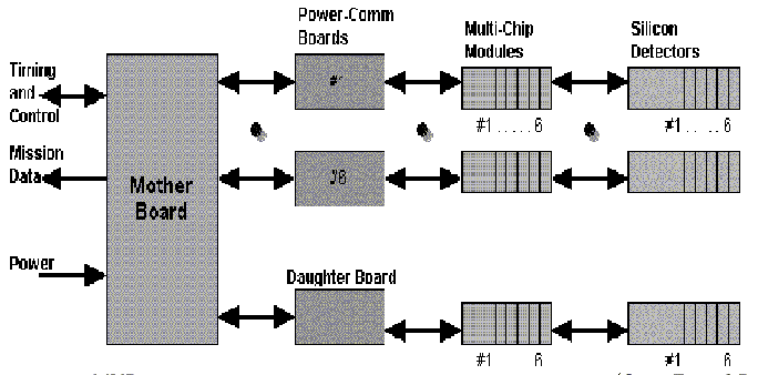
Figure 1. Block diagram of MVD front-end electronics
----------------------------------------------------------------------
Sangkoo Hahn, LeRoy Cope, Jan Boissevain and Gary Smith
31 July 98
PHENIX-MVD-98-21, PHENIX Note 350
1. Introduction
The four motherboards inside the MVD perform the electrical and mechanical equivalent of a backbone for the system. The main functions of the motherboards are;

Figure 1. Block diagram of MVD front-end electronics
2. Mechanical Arrangement
There are two types of motherboards, Left and Right. Two motherboards per each type are used for the MVD due
to the plane-symmetry of the detector arrangement. (Go to
this
reference for a more comprehensive review of the mechanical
setup of MVD.) The two motherboard types are identical in electrical functions, so the layout is based on the
same schematics. However, the layout, ideally a mirroring of one type to the other, has to take into account all
components such as connectors and active devices, which have no mirroring pin orientations.
As shown in Figure 1 above, six power-communication (power-comm for short) boards and one daughter board plug into each motherboard. The six power-comm boards are parallel to each other when plugged into the motherboard. The daughter board, holding pad detectors at the end of the cylindrical body of the MVD, is connected to the motherboard away from the power-comm board. The cable connectors interfacing with the main power supplies and the interface modules are on the backside of the motherboard away from the power- comm boards.
3. Power Regulations and Distributions
3.1 Five different voltages are used in the front-end electronics; +5VD (digital), +5VA_TGV (analog, preamp), -
5VA (analog, preamp), +5VA_Comp (analog, comparator), +2.5VA (analog, bias). In addition, a silicon bias
voltage of approximately 50V is passed through the motherboard. Seven sets of five voltages are supplied to
the six groups of power-comm boards and a daughter board through Low Drop-Out (LDO) voltage regulators
(MIC29XX0-type) as shown below. Each input is fused and each output has both ceramic and electrolytic
capacitors to supply returns.
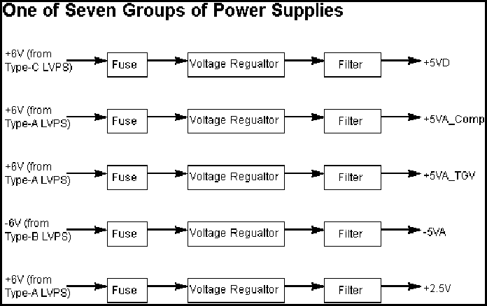
Figure 2. Power regulation and filtering for each voltage rail.
3.2 Power Consumption. (The following estimates are just estimates. Further testing and estimates are required to arrive at more accurate figures.)
The power consumption of the motherboard itself is as follows.
| +5VD | 0.2A | 1.0W |
| +5VA | (negligible) | (negligible) |
| -5VA | (negligible) | (negligible) |
| Total of 1W (for one motherboard only) |
The power estimates for one power-comm board with 6 MCM's connected are;
| +5VD | 1. 4A | 7W |
| +5VA_TGV | 0 .6A | 3W |
| +5VA_Comp, etc | 0 .8A | 4W |
| -5VA | 0.2A | 1W |
| +2.5VA | (small) | (negligible) |
| Total of 15W (for one power-comm board and 6 MCMs) | ||
The estimated power consumption for each motherboard and all front-end electronics connected to it are as follows. The regulator head voltages (the amount of voltage drop as the current passes through the regulator) are fixed at 1.0V for convenience.
| +5VD: | 50W |
| +5VA (both preamp and comparator): | 50W |
| -5VA (both preamp and comparator): | 9W |
| +2.5V: | (negligible) |
| +50V Si-Bias: | (negligible) |
| Total of 109W per one motherboard, or Total of 436W for the whole MVD |
3.3 All 38voltage regulator input lines were fused with resettable fuses (Poly-Fuse model SMD250 by Raychem). All of the poly-fuses are rated for 2.5A current at 20 degrees C.
4. Timing and Control Signals
As a main function, the motherboard distributes timing and control signals throughout the front-end electronics. Most high-speed signals such as beam clocks and mode bits do not originate nor terminate on the motherboard. However, one of the seven 4 x beam clock signals going to the Power-Comm and Daughter boards is tapped off the pass-through signal to create the PECL (Positive ECL) clocks for all MCMs. PECL logic clock is used for the AMUADCs on MCMs for low interference to the sensitive preamp inputs as it has small and smooth voltage swings and balanced current spikes.
(Note: For logic signals with fast edges, ACT-logic is used with 22-ohm series resistor at the source end and 51- ohm termination resistor on the receiver side. Other logic signals with slow edges such as serial clocks for MCM programming and serial controls for monitors use un-terminated AC-logic.)
5. LVDS data and pass-through signals
The mission data packets from each MCM are transmitted through the motherboard using low voltage differential signal lines. These lines, however, are just passed through without any buffering as the LVDS line drivers (90C031) on the power-comm board handles the signals. Other pass-through data lines as shown in the figure below include the current-sum signals, silicon bias voltages, the serial control and serial data to/from the MCM and the mode-bits. Fast pass-through signals were given special attention for signal integrity during the board layout for better high-frequency performance as explained later.
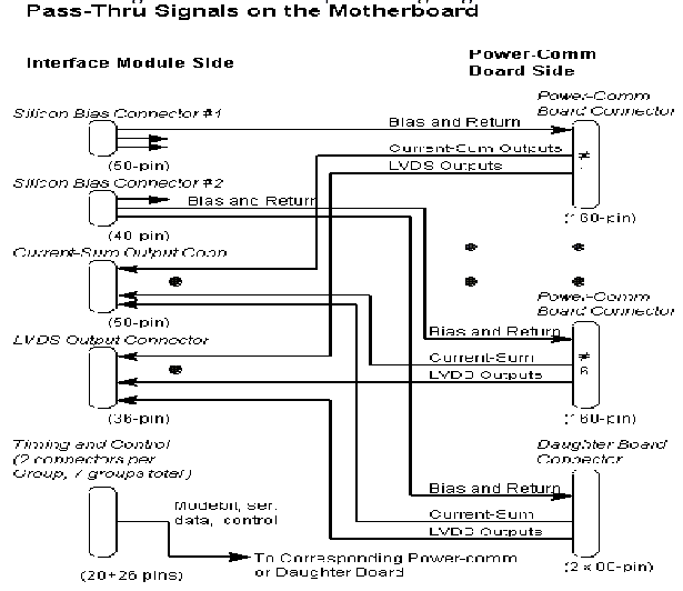
Figure 3. Motherboard pass-through signals
6. The spy channels, temperature and voltage monitors.
The spy channel analog voltage information is multiplexed and buffered on the motherboard to send to interface module. The frequency bandwidth of the signal is not relatively narrow, and OP283 by Analog Devices was chosen as the buffer. Six multiplexers (ADG406 by Analog Devices) with 16 channels each are addressed by 6-bit selection lines, 2 bits of which is decoded locally to select 1of the 6 chips.
There are 93 analog monitor lines on the motherboard for all power supply voltages and temperatures. 12 of MAX186 8-channel multiplexer with built-in analog-to-digital converters are used for 96 total channels including three spares. The chip selection is done through 4-to-16 decoder while channel selection and conversion controls are done through serial control data.
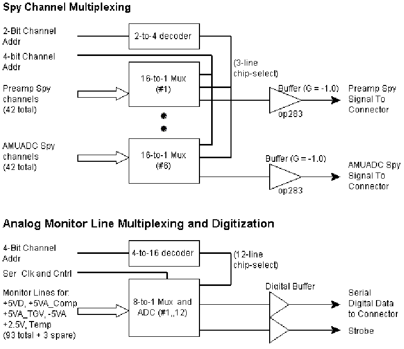
Figure 4. Multiplexing and control of the analog monitor signals
7. PCB Layout
The most important layout feature, in addition to the fact that it has to fit within a very tight MVD enclosure, is to keep the signal integrity of the fast signals as they travel through the length of the traces on the board. The LVDS signals from each of the MCMs carry the mission data on a 4 x beam clock rate, and has the characteristic line impedance controlled to approximately 50 ohms by using 5-mil thick FR-4 printed circuit board material and 7-mil trace and spacing.
Similar impedance control is maintained for the clock lines of 9.5 MHZ and 38MHz at CMOS levels, and 38 MHz-PECL lines.
With 38 power regulators on the motherboard, it was important to conduct the heat away from the MVD enclosure through a cooling coil in thermal contact with the regulator body. The motherboard layout included copper pads for the regulator body as well as thermal vias to the backside of the board where the cooling pipe is routed.
8. Connector Pin Assignments for the Motherboard.
For a complete listing of signal assignments for connector pins on the motherboard, please go to this reference, and click on the "MVD Signals."
9. Test Plan for the Motherboard
9.1 Component placement and assembly quality
9.2 Voltage regulators
Equipment required: dual output DC power supply with outputs of +/- 6.5V or greater, one oscilloscope, one power input connector , one Panduit CT156F18-14DA , all wired as per motherboard schematic sheet #2,
9.3 PECL differential clock line
Equipment required: one pulse generator with better than 40MHz repetition rate, one oscilloscope
9.4 Spy channel multiplexer and buffer amplifier
Equipment required: One analog signal generator, one oscilloscope, and one data generator to address multiplexer channels
| SPY_A5 | A4 | A3 | A2 | A1 | A0 | SELECTS (x = don't care) |
| x | x | 0 | 0 | 0 | 0 | S0 |
| x | x | 0 | 0 | 0 | 1 | S1 |
| x | x | 0 | 0 | 1 | 0 | S2 |
| x | x | 0 | 0 | 1 | 1 | S3 |
| x | x | 0 | 1 | 0 | 0 | S4 |
| x | x | 0 | 1 | 0 | 1 | S5 |
| x | x | 0 | 1 | 1 | 0 | S6 |
| x | x | 0 | 1 | 1 | 1 | S7 |
| x | x | 1 | 0 | 0 | 0 | S8 |
| x | x | 1 | 0 | 0 | 1 | S9 |
| x | x | 1 | 0 | 1 | 0 | S10 |
| x | x | 1 | 0 | 1 | 1 | S11 |
| x | x | 1 | 1 | 0 | 0 | S12 |
| x | x | 1 | 1 | 0 | 1 | S13 |
| x | x | 1 | 1 | 1 | 0 | S14 |
| x | x | 1 | 1 | 1 | 1 | S15 |
| 0 | 0 | x | x | x | x | U71,U68 |
| 0 | 1 | x | x | x | x | U70,U67 |
| 1 | 0 | x | x | x | x | U69,U66 |
9.5 Multiplexer ADC and serial output data
Equipment required : One pattern generator (to generate 24 bit sequence to select one of eight analog input channels and initiate an analog to digital conversion,) an analog signal generator, one oscilloscope. (Note: One way of addressing the serial ADC is to use a bank of switches switching between +5v and ground, with a debounce circuit.)
a. Quick look: The objective of this test is to quickly evaluate the analog performance without the pattern
generator. A quick look at ADC operation could be done by addressing the MAX186 ADC chip by clocking in all
logic level-1.
(Refer to J23 on sheet two of mother board schematic. Signals involved are MON_SER_CLK,
MON_SER_DATA_IN, and MON_SER_DATA_OUT)
The chip-select address bit combinations and selected chips are as follows.
| ADC_A3 | ADC_A2 | ADC_A1 | ADC_A0 | SELECTS |
| 0 | 0 | 0 | 0 | U1 |
| 0 | 0 | 0 | 1 | U2 |
| 0 | 0 | 1 | 0 | U3 |
| 0 | 0 | 1 | 1 | U4 |
| 0 | 1 | 0 | 0 | U5 |
| 0 | 1 | 0 | 1 | U6 |
| 0 | 1 | 1 | 0 | U7 |
| 0 | 1 | 1 | 1 | U8 |
| 1 | 0 | 0 | 0 | U9 |
| 1 | 0 | 0 | 1 | U10 |
| 1 | 0 | 1 | 0 | U11 |
| 1 | 0 | 1 | 1 | U12 |
The serial control bit combinations and their functions are as follows.
SERIAL_CONTROL_BYTE (MSB first, x = don�t care)
| MSB | LSB | ||||||||
| 7 | 6 | 5 | 4 | 3 | 2 | 1 | 0 | Function | |
| x | x | x | x | x | x | 0 | 0 | Full power down | |
| x | x | x | x | x | x | 0 | 1 | Fast power down | |
| x | x | x | x | x | x | 1 | 0 | Internal clock mode | |
| x | x | x | x | x | x | 1 | 1 | Ex | ternal clock mode |
| x | x | x | x | x | 1 | x | x | single ended inputs | |
| x | x | x | x | 1 | x | x | x | unipolar | |
| x | 0 | 0 | 0 | x | x | x | x | CH0 | |
| x | 0 | 0 | 1 | x | x | x | x | CH1 | |
| x | 0 | 1 | 0 | x | x | x | x | CH2 | |
| x | 0 | 1 | 1 | x | x | x | x | CH3 | |
| x | 1 | 0 | 0 | x | x | x | x | CH4 | |
| x | 1 | 0 | 1 | x | x | x | x | CH5 | |
| x | 1 | 1 | 0 | x | x | x | x | CH6 | |
| x | 1 | 1 | 1 | x | x | x | x | CH7 | |
| 1 | x | x | x | x | x | x | x | Start |
9.6 Pin-to-pin resistance tests for pass-through signals
This test is to ensure the connectivity of all the pass-through signals from a pin on one connector to another pin on another connector through a printed circuit trace. These signals are LVDS, Current _Sum, Silicon Bias Voltages, and Digital and Analog Grounds (signal commons). The test is performed by connecting an ohm-meter between the designated pins on two connectors as identified by the following lists. The DC resistance should be less than 3.0-Ohm
--------------------------------------------------------------------------------------------------------------------- The signals listed below are common to each group. (Refer to the GROUP TABLE for reference designator information.)
| TIM/CONT | POWER/COMM | |
| GROUP TABLE | CONN xx | CONN yy |
| GROUP 1 | J9 | to J41 |
| GROUP 2 | J10 | to J40 |
| GROUP 3 | J11 | to J39 |
| GROUP 4 | J12 | to J38 |
| GROUP 5 | J13 | to J37 |
| GROUP 6 | J14 | to J36 |
| GROUP 7 | J15 | to J35 |
| | ||
| SIGNAL | PIN | PIN |
| (n = 1 thru 7) | xx | yy |
| Gn_MB0 | 1 | 1 |
| Gn_MB1 | 3 | 2 |
| Gn_MB2 | 5 | 3 |
| Gn_MB3 | 7 | 4 |
| Gn_MB4 | 9 | 5 |
| Gn_MB5 | 11 | 6 |
| Gn_L1A | 13 | 9 |
| DGND | 2 | 11,12 |
| DGND | 4 | 11,12 |
| DGND | 6 | 11,12 |
| DGND | 8 | 11,12 |
| DGND | 10 | 11,12 |
| DGND | 12 | 11,12 |
| DGND | 14 | 11,12 |
| DGND | 16 | 11,12 |
| DGND | 18 | 11,12 |
| DGND | 19 | 11,12 |
| DGND | 20 | 11,12 |
| ----------------------------------------------------- | ||
| GROUP 1 | J28 | J41 |
| GROUP 2 | J29 | J40 |
| GROUP 3 | J30 | J39 |
| GROUP 4 | J31 | J38 |
| GROUP 5 | J32 | J37 |
| GROUP 6 | J33 | J36 |
| GROUP 7 | J27 | J35 |
| SIGNAL | PIN | PIN |
| Gn_MCM1_S_EN | 3 | 55 |
| Gn_MCM2_S_EN | 4 | 56 |
| Gn_MCM3_S_EN | 5 | 57 |
| Gn_MCM4_S_EN | 6 | 58 |
| Gn_MCM5_S_EN | 7 | 59 |
| Gn_MCM6_S_EN | 8 | 60 |
| Gn_SERIAL_CLK | 11 | 63 |
| Gn_S_DATA_OUT_MCM1 | 15 | 67 |
| Gn_S_DATA_OUT_MCM2 | 16 | 68 |
| Gn_S_DATA_OUT_MCM3 | 17 | 69 |
| Gn_S_DATA_OUT_MCM4 | 18 | 70 |
| Gn_S_DATA_OUT_MCM5 | 19 | 71 |
| Gn_S_DATA_OUT_MCM6 | 20 | 72 |
| Gn_S_LATCH | 21 | 75 |
| Gn_READBACK_EN | 22 | 76 |
| Gn_XILINX_PROGRAM | 25 | 77 |
| Gn_MCM_RESET | 26 | 78 |
| -----All Digital and Analog Ground pins should be shorted together between themselves. | ||
| DGND | 1 | 53 |
| DGND | 2 | 54 |
| DGND | 9 | 61 |
| DGND | 10 | 62 |
| DGND | 13 | 65 |
| DGND | 14 | 66 |
| DGND | 23 | 73 |
| DGND | 24 | 74 |
| DGND | J23-1, 2, 4, 6, 11, | |
| J23-13, 17, 18, | ||
| J23-25, 26, 27, 28 | ||
| DGND | 11, 12, 101, 102, 105, 109, 113, 117, 121, 125, | |
| 129, 133, 137, 141 | ||
| AGND | J23-31, 32, 35, | |
| J23-36, 39, 40 | ||
| AGND | 80,93,94,110,114,118,122,126 | |
| ------------ Group 7 is a special case [Uses two 80-pin connectors instead of one 160-pin.] | ||
| DGND | J35-11, 12, 53, 54, 61, 62, 65, 66, 73, 74, | |
| J34-21, 22, 25, 29, 33, 37, 41, 45, 49, 53, 57, 61 | ||
| AGND | J35-80 | |
| J34-13, 14, 26, 30, 34, 38, 42, 46 | ||
| AGND | J26-2, 4, 6, 8, 10, 12, 14, 16, 18, 20, 22, 24, | |
| J26-28, 30, 32, 34, 36, 38, 40, 44, 46, 48 | ||
| ---------------------Current Sum Output----------------------- | ||
| G1_MCM1_DS | J26-1 | J41-95 |
| G1_MCM2_DS | J26-3 | J41-96 |
| G1_MCM3_DS | J26-5 | J41-97 |
| G1_MCM4_DS | J26-7 | J41-98 |
| G1_MCM5_DS | J26-9 | J41-99 |
| G1_MCM6_DS | J26-11 | J41-100 |
| G2_MCM1_DS | J26-13 | J40-95 |
| G2_MCM2_DS | J26-15 | J40-96 |
| G2_MCM3_DS | J26-17 | J40-97 |
| G2_MCM4_DS | J26-19 | J40-98 |
| G2_MCM5_DS | J26-21 | J40-99 |
| G2_MCM6_DS | J26-23 | J40-100 |
| G3_MCM1_DS | J26-25 | J39-95 |
| G3_MCM2_DS | J26-27 | J39-96 |
| G3_MCM3_DS | J26-29 | J39-97 |
| G3_MCM4_DS | J26-31 | J39-98 |
| G3_MCM5_DS | J26-33 | J39-99 |
| G3_MCM6_DS | J26-35 | J39-100 |
| G7_MCM1_DS | J26-37 | J34-15 |
| G7_MCM2_DS | J26-39 | J34-16 |
| G7_MCM3_DS | J26-41 | J34-17 |
| G7_MCM4_DS | J26-43 | J34-18 |
| G7_MCM5_DS | J26-45 | J34-19 |
| G7_MCM6_DS | J26-47 | J34-20 |
| ---------------------- SI-Detector Bias------------------------- | ||
| G1_MCM1_SB | J24-1 | J41-149 |
| G1_MCM1_SBR | J24-2 | J41-150 |
| G1_MCM2_SB | J24-3 | J41-151 |
| G1_MCM2_SBR | J24-4 | J41-152 |
| G1_MCM3_SB | J24-5 | J41-153 |
| G1_MCM3_SBR | J24-6 | J41-154 |
| G1_MCM4_SB | J24-7 | J41-155 |
| G1_MCM4_SBR | J24-8 | J41-156 |
| G1_MCM5_SB | J24-9 | J41-157 |
| G1_MCM5_SBR | J24-10 | J41-158 |
| G1_MCM6_SB | J24-11 | J41-159 |
| G1_MCM_SBR | J24-12 | J41-160 |
| | ||
| G2_MCM1_SB | J24-13 | J40-149 |
| G2_MCM1_SBR | J24-14 | J40-150 |
| G2_MCM2_SB | J24-15 | J40-151 |
| G2_MCM2_SBR | J24-16 | J40-152 |
| G2_MCM3_SB | J24-17 | J40-153 |
| G2_MCM3_SBR | J24-18 | J40-154 |
| G2_MCM4_SB | J24-19 | J40-155 |
| G2_MCM4_SBR | J24-20 | J40-156 |
| G2_MCM5_SB | J24-21 | J40-157 |
| G2_MCM5_SBR | J24-22 | J40-158 |
| G2_MCM6_SB | J24-23 | J40-159 |
| G2-MCM6_SBR | J24-24 | J40-160 |
| | ||
| G3_MCM1_SB | J24-25 | J39-149 |
| G3_MCM1_SBR | J24-26 | J39-150 |
| G3_MCM2_SB | J24-27 | J39-151 |
| G3_MCM2_SBR | J24-28 | J39-152 |
| G3_MCM3_SB | J24-29 | J39-153 |
| G3_MCM3_SBR | J24-30 | J39-154 |
| G3_MCM4_SB | J24-31 | J39-155 |
| G3_MCM4_SBR | J24-32 | J39-156 |
| G3_MCM5_SB | J24-33 | J39-157 |
| G3_MCM5_SBR | J24-34 | J39-158 |
| G3_MCM6_SB | J24-35 | J39-159 |
| G3_MCM6_SBR | J24-36 | J39-160 |
| | ||
| G4_MCM1_SB | J24-37 | J38-149 |
| G4_MCM1_SBR | J24-38 | J38-150 |
| G4_MCM2_SB | J24-39 | J38-151 |
| G4_MCM2_SBR | J24-40 | J38-152 |
| G4_MCM3_SB | J24-41 | J38-153 |
| G4_MCM3_SBR | J24-42 | J38-154 |
| G4_MCM4_SB | J24-43 | J38-155 |
| G4_MCM4_SBR | J24-44 | J38-156 |
| G4_MCM5_SB | J24-45 | J38-157 |
| G4_MCM5_SBR | J24-46 | J38-158 |
| G4_MCM6_SB | J24-47 | J38-159 |
| G4_MCM6_SBR | J24-48 | J38-160 |
| | ||
| G5_MCM1_SB | J25-1 | J37-149 |
| G5_MCM1_SBR | J25-2 | J37-150 |
| G5_MCM2_SB | J25-3 | J37-151 |
| G5_MCM2_SBR | J25-4 | J37-152 |
| G5_MCM3_SB | J25-5 | J37-153 |
| G5_MCM3_SBR | J25-6 | J37-154 |
| G5_MCM4_SB | J25-7 | J37-155 |
| G5_MCM4_SBR | J25-8 | J37-156 |
| G5_MCM5_SB | J25-9 | J37-157 |
| G5_MCM5_SBR | J25-10 | J37-158 |
| G5_MCM6_SB | J25-11 | J37-159 |
| G5_MCM6_SBR | J25-12 | J37-160 |
| | ||
| G6_MCM1_SB | J25-13 | J36-149 |
| G6_MCM1_SBR | J25-14 | J36-150 |
| G6_MCM2_SB | J25-15 | J36-151 |
| G6_MCM2_SBR | J25-16 | J36-152 |
| G6_MCM3_SB | J25-17 | J36-153 |
| G6_MCM3_SBR | J25-18 | J36-154 |
| G6_MCM4_SB | J25-19 | J36-155 |
| G6_MCM4_SBR | J25-20 | J36-156 |
| G6_MCM5_SB | J25-21 | J36-157 |
| G6_MCM5_SBR | J25-22 | J36-158 |
| G6_MCM6_SB | J25-23 | J36-159 |
| G6_MCM6_SBR | J25-24 | J36-160 |
| | ||
| G7_MCM1_SB | J25-25 | J34-69 |
| G7_MCM1_SBR | J25-26 | J34-70 |
| G7_MCM2_SB | J25-27 | J34-71 |
| G7_MCM2_SBR | J25-28 | J34-72 |
| G7_MCM3_SB | J25-29 | J34-73 |
| G7_MCM3_SBR | J25-30 | J34-74 |
| G7_MCM4_SB | J25-31 | J34-75 |
| G7_MCM4_SBR | J25-32 | J34-76 |
| G7_MCM5_SB | J25-33 | J34-77 |
| G7_MCM5_SBR | J25-34 | J34-78 |
| G7_MCM6_SB | J25-35 | J34-79 |
| G7_MCM6_SBR | J25-36 | J34-80 |