 length of the interaction region. The vertex position resolution is better than 200
 , limited by the 200 pitch of the silicon strips. This is more than adequate for the muon and central tracking use.s ADC. The system controller or Heap Manager, supplies all timing control, data buffering, and data formatting for a single 256-channel multi-chip module (MCM). Each chip set is partitioned into 32-channel sets. Prototype performance for the various blocks will be presented as well as the ionizing radiation damage performance of the 1.2 nwell CMOS process used for fabrication.
The vertex position is located using hits in the barrel for Z position between -40 and +40 cm, which covers the 2 length of the interaction region. The vertex position resolution is better than 200, limited by the 200 pitch of the silicon strips. This is more than adequate for the muon and central tracking use.
The multiplicity trigger is formed using the sum of silicon channels (both pads and strips) above a threshold corresponding to approximately 0.25-0.33 of a minimum ionizing particle (MIP). For off-line analysis of the charged particle multiplicity and fluctuations over 5 units of rapidity, the pulse height from each channel will be used to separate multiple from single hits. In a single event, the MVD is sensitive to multiplicity fluctuations at the 10% level; this is limited by backgrounds and charged particle statistics rather than MVD performance.
This paper presents measurements of the prototype component systems of the MVD detector electronics. The circuits include the preamplifier-discriminator, analog memory unit (AMU), analog-digital converter (ADC), and heap manager.
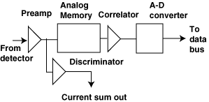
Figure 1. System block diagram.
The electronics will be mounted on multi-chip modules (MCM). Each MCM will be connected to 256 detectors and will contain 8 preamplifier-discriminator chips and 8 analog memory-ADC chips. Each of these chips will contain 32 channels of their respective functions. In addition, the MCM will contain the Heap Manager chips and associated control logic. The present prototype chips are 8 channels of respective functions.
A. The drain current curve is shown in Fig. 3. The PHENIX and PHOBOS versions employ wideband gain stages after the preamplifier because the output will be processed by a correlated sampler. The NRL version employs a semi-Gaussian shaper with 7s peaking time. A summary of the performace of the three versions is presented in Table 1. The resultant power dissipation of the PHENIX preamplifier with the gain stages is approximately 1.2mW. The circuit is fabricated in 1.2 n-well CMOS and has a pitch of 85.
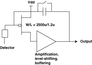
Figure 2. MVD preamplifier
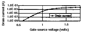
Figure 3. Drain current vs. Vgate-source
| Parameter | PHENIX (224ns double correlated) | PHOBOS (Wideband) | NRL (7s peaking) |
|---|---|---|---|
| 0pF noise | 660e | 750e | 205e |
| Slope | 69e/pF | 30e/pF | 3e/pF |
| Gain | 44mV/fC | 4.2mV/fC | 11mV/fC |
| Drain | 100A | 200A | 100A |
| current |
Table 1. Performance of various preamplifer versions.
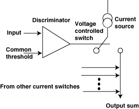
Figure 4. Block diagram of the discriminator
The summed currents are input to an on-MCM opamp that converts the current to a voltage which is then run off of the MCM to a pipelined flash ADC for conversion of the trigger sum. The design allows triggering at every beam crossing (112ns intervals) with no deadtime. The total power consumption is approximately 500W/channel. A plot of the output is shown in Fig. 5.
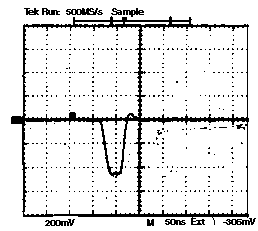
Figure 5. Discriminator output
C. Analog memory-correlator
The analog memory unit (AMU) is a 64-cell deep, voltage-write-voltage-read, deadtime-less topology with a power dissipation of approximately 1mW/channel. The memory is followed by an analog correlator that performs the double-correlated sampling. Both direct memory output and correlated output are available to the subsequent analog-digital converter (ADC). The memory reading and writing is addressed externally from the Heap Manager. The read and write logic decoders are completely independent to allow simultaneous read-write (deadtime-less) operation. A block diagram of the memory is presented in Fig. 6.
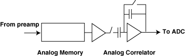
Figure 6. Memory block diagram
The analog-digital converter (ADC), presented in Fig. 7, is a 10-bit Wilkinson type [2] with a maximum dynamic range of 4.5 Volts. This prototype has eight channels.
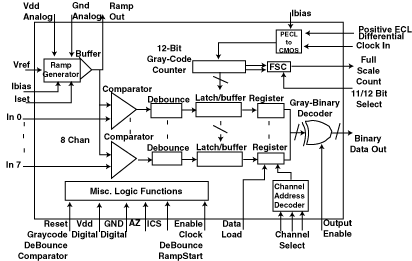
Figure 7. Block diagram of ADC chip.
The Gray code counter uses a positive ECL logic level differential clock input with frequencies as high as 212 Mhz. A Gray code counter circuit is used for two reasons: first, since only one bit changes at a time, transient currents should be smaller, consequently making noise levels lower. Second, any single-bit error in transmission will result in only an LSB magnitude error. The Gray-coded data passes through a Grapy-to-binary conversion circuit when the chip data is read out. There is also a one-word deep memory on the chip to allow readout of data from one conversion while another conversion is taking place.
The ramp generation circuit consists of an operational amplifier with an on-chip feedback capacitor to form an integrator. This provides a low output impedance ramp signal that is not affected by loading from multiple ADC channels on the same chip. The ramp and comparator circuits use a separate analog power and ground connection from the rest of the digital sections of the chip for isolation.
The ADC uses 3.75W/MHz/channel in the digital circuitry and 6.5mW total in the ramp generator. This results in a power dissipation of approximately 0.6mW/channel for a 32-channel chip or 1.19mW/channel for the 8-channel prototype at 100MHz clock frequency (5s conversion time for 10-bit conversions). At 144 Mhz clock rate and 10 bits, the Integral Nonlinearity (INL) is about +/-0.1% of full scale. Full Width Half Max (FWHM) is less than 2 bins wide at higher input voltages and deteriorates to about 6 bins at low input voltages. The cause of this has not been determined at this time.
A generic heap manager has been developed for use in all PHENIX detector subsystems using analog memory for front-end signal buffering during the Level-1 trigger decision. However, due to the reduced size and power requirements for the MVD, this functional block has been partitioned such that the minimum required electronics are physically located near the detectors. The remaining circuitry resides at the ends of the detector subassembly as interface cards to the data collection modules (DCMs). Figure 8 is a block diagram of the MVD heap manager showing the basic functional blocks and system partitioning.
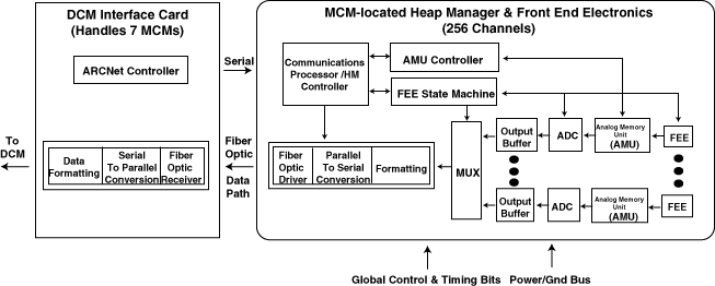
Figure 8. Block Diagram of the Heap Manager
CMOS process were made. Versions of the preamplifier, analog memory and ADC circuits have been irradiated to various doses of ionizing radiation. The process appears to be sufficient for doses up to greater than 75krad for most functions. The major problem is in the leakage current of the input protection for the preamplifier. Devices used for protection networks begin to exhibit increased leakage current due to the radiation-induced decrease in the nmos threshold voltage. We are continuing to investigate improved input protection. Figure 9 is a plot of the analog memory unit Integral Non-Linearity (INL) for various doses of 60Co.
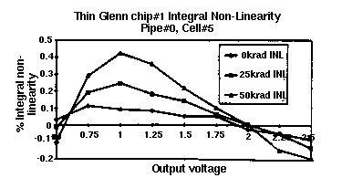
Figure 9. Amu integral-nonlinearity for various radiation doses.