Design and Characterization of the BVX: An 8-Channel CMOS Preamplifier-Shaper
for Silicon Strips
C. L. Britton, Jr., G. T. Alley, M. L. Simpson, A. L. Wintenberg, R. J. Yarema, T. Zimmerman,
J. Boissevain, W. Collier, B. V. Jacak, J. Simon-Gillo, W. Sondheim, J. P. Sullivan, and N. Lockyer*
Published in IEEE Transactions on Nuclear Science, Vol. 41, No. 1, February, 1994.
PHENIX-MVD-94-3
PHENIX Note #221
Abstract-This paper presents the design and characterization of an 8-channel preamplifier-shaper intended for use with silicon strip detectors ranging in capacitance from 1 to 20 pF. The nominal peaking time of the circuit is 200 ns with an adjustment range of  50 ns. The circuit has a pitch (width) of 85
  m/channel with a power dissipation of 1.2 mW/channel and has been fabricated in 2
  m p-wells CMOS. The 0 pF noise is 330 e with a noise slope of 64 e/pF. The design approach is presented as well as both test bench and strip detector measurements.
I. Introduction
The original application for this preamplifier-shaper, called the BVX for bottom vertex, was for use in the bottom collider detector (BCD) at Fermilab, but the circuit is presently being used for silicon strip detector evaluation for the PHENIX detector at RHIC. The nominal peaking time is 200 ns with an adjustment range of at least  50 ns for compatibility with the proposed Tevatron upgrade (400 ns interaction rate) and a circit pitch of 85
  m for compatiblity with 100
  m pitch silicon strip detectors. An 8-channel device was fabricated to study channel uniformity and crosstalk, but the design is easily expanded to 64 or 128 channels as required. The power dissipation is 1.2 mW per channel.
One requirement of this circuit was a conversion gain of greater than 50 mV/fC. This was to minimize the effect of offset nonlinearities in a subsequent analog memory array. The circuit as fabricated has a conversion gain of approximately 75 mV/fC for a 0 pF detector capacitance. The shaping is approximately CR-RC3 which allows a return to baseline within 2 beam crossings (800 ns). The chosen topology for the preamplifier is that of the folded cascode with a long NMOS feedback resistor to allow compensation of detector leakage current [1]. Because of the high conversion gain and multi-pole shaping, a topology comprised of two differential amplifiers was chosen. All poles are real and the time response is unipolar without the resultant undershoot often exhibited by filters using complex poles.
A description of the circuitry will be presented with comparisons between simulated and fabricated circuits. Noise, gain and offset measurements of the actual circuits and description of present use will also be presented.
II. Circuit Description
The preamplifier, shown in Fig. 1, is a folded cascode topology using a long channel NMOS transistor for the feedback resistor [1]. The input transistor is a PMOS device operating at a drain current of 100  A with a width/length (W/L) value of 1080
  m/2
m/2  m. A common problem with folded cascode designs is the noise generated by second-stage biasing circuits. To reduce this noise, two circuit techniques are used in this design. The first is the use of a filter capacitor on the gates of the current sources. HSPICE simulations indicate that the presence of M15 improves the noise amplitude by approximately 23% for a 10 pF detector capacitance. A transistor is used as the capacitor which provides more than a 60% increase in capacitance compared to a double poly capacitor of the same approximate area. The second technique used to lower the noise is the use of source degenerated current mirrors for biasing. The use of transistors M7 (W/L = 100
  m/20
m/20  m) and M8 (W/L = 10
  m/20
m/20  m) biased in the deep ohmic region as resistors at the sources of the driver M5 (W/L = 10
  m/10
m/10  m) and mirror M4 (W/L = 100
  m/10
m/10  m) improves the noise amplitude approximately 5% over sizing M4 and M5 with the same width, but with a length of 30
  m. This increase in length would make the overall area of the mirror pair approximately the same as with the degeneration. Source degeneration was also applied to the mirror set of M3 and M6. The risetime of the preamplifier (with an input capacitance of approximately 3 pF) is 100 ns.
The first and second shapers are differential amplifier stages with bandwidth control to implement the shaping.

Fig 1. Preamplifier schematic.
A long channel NMOS transistor, M28, is used to adjust the peaking time by setting the location of the pole. The third stage shaper is primarily a gain-filter stage that is also buffered for off-chip drive. The third stage feedback resistors were implemented as strips of p-well. The first and second shaper schematic diagrams are shown in Figs. 2 and 3.
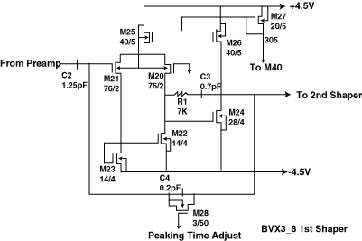
Fig 2. First shaper schematic
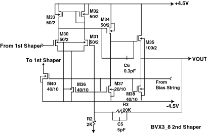
Fig 3. Second shaper schematic.
III. Noise Measurements
The noise measurements, presented in Table 1, were made on bare die mounted on a circuit board.
| Cin (pF) | Simulated ENC(e) | Measured ENC(e) |
|---|
| 0 | 180 | 330 |
| 1 | - | 400 |
| 5 | - | 700 |
| 10 | 810 | 970 |
| 20 | - | 1620 |
Table 1: Noise Versus Input Capacitance
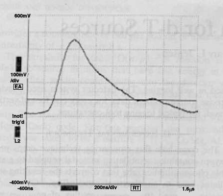
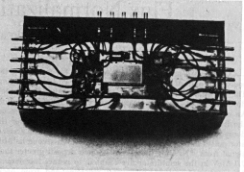
We believe that there are three possible reasons for the differences between the simulated and measured noise. First, transconductance has been found to be overestimated by the vendors models, particularly since the input device of this preamplifier is operating between weak and strong inversion, a difficult region to model. Second, the series noise in large geometry devices has been found to be higher than predicted by SPICE [2]. Third, even though the simulation included the additional bonding pad and input wiring capacitance (which is approximately 0.5 pF), these are estimates and not measured values. We therefore suspect that the stray capacitance at the input is actually higher since the differences between simulated and measured at both 0 pF and 10 pF are approximately 160 e. This would indicated a stray of 2-3 pF. An oscilloscope photo of the output waveform of the preamplifier is shown in Fig. 4. A photograph of the chip is shown in Fig. 5.
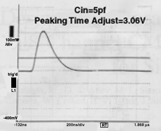
Fig 4. Oscilloscope photo of the output waveform.

Fig 5. Die photo of the BVX
IV. Performance Summary
A summary of all eight channels on one chip is given in Table II. The measurement parameters are Cin = 10 pF, Qin = 5 fC. Peaking time is controlled by a voltage on the peaking time adjust input pin which was equal to +2.25 V for this test. The mean value of the output offset is 63.6 mV and  (standard deviation) is 51.2 mV. The high value of
  is partly due to the layout. The differential input devices of the first and second stage shapers have both small gate areas [3] and, due to the tight space requirements, a layout that is not common centroid geometry [4]. Although the magnitude is not surprising, the variation is disappointing since the reason for the differential designs is to allow both the amplifier pedestal and the subsequent analog memory pedestal to be much less than 1 fC. Given the high conversion gain, this would allow the electronic pedestal to be virtually ignored. Since the output of the second shaper is not designed for off-chip drive, a 47K resistor from the output to the negative supply was added to enhance drive in the presence of excess capacitance for the following measurements.
| Channel | Peaking
time(ns) | Gain
(mV/fC) | ENC(e) | Vout
dc(mV) |
|---|
| 1 | 240 | 79.3 | 900 | +43 |
| 2 | 244 | 79.0 | 920 | +126 |
| 3 | 248 | 79.8 | 910 | +35 |
| 4 | 244 | 78.6 | 900 | +109 |
| 5 | 244 | 77.6 | 880 | +68 |
| 6 | 236 | 76.4 | 900 | -42 |
| 7 | 240 | 78.4 | 910 | +114 |
| 8 | 244 | 81.0 | 930 | +56 |
Table II: 8-Channel Performance Summary (Chip#2)
The matching between two chips is shown in Table III.
The chip-to-chip matching is obviously not as good as the channel-to-channel matching on a given chip. For example, the worst case spread for peaking time varies from 212 ns on chip#1 to 248 ns on chip#2, a difference of 17%. Within some range, however, the spread may be completely acceptable for a given application. The dynamic range of the amplifier is from 0 to +28 fC and 0 to -10 fC with a 4% integral linearity error between +5 fC and +20 fC. The dynamic range is limited by the linear range of the source-follower output stage. The very high conversion gain of this preamplifier corresponds to approximately 7 minimum ionizing particles (MIP) for positive output excursions. This may be increased by decreasing the gain of the preamplifier at the cost of lower conversion gain, but should be adequate for most applications. The adjacent channel crosstalk is approximately 1%. The peaking time was found to increase by 10 ns for a 1 V output and 20 ns for a 2 V output. This was thought to be due to nonlinearities in the large signal response of the second shaper stage. The peaking time was found to vary from 220 ns for Cin = 10 pF to 252 ns for Cin = 20 pF for a fixed peaking-time adjust value of 2.25 V. Peaking-time control voltage vs. time and gain are presented in Table IV. The nominal range of adjustment was found to be approximately  50 ns which was found to give more than sufficient adjustment for chip-to-chip variations in peaking time. Since the primary use of the BVX was for a 200 ns peaking time system, noise for the other values of peaking time was not measured.
| Chip # | Peaking
time(ns) | Gain
(mV/fC) | ENC(e) | Vout
dc(mV) |
|---|
| 1 | x = 215, | x = 74, | x = 947, | x = 93, |
| |  = 4 = 4 |  = 0.94 = 0.94 |  = 27.1 = 27.1 |  = 123 = 123 |
| 2 | x = 243, | x = 78.8, | x = 906, | x = 63.6, |
| |  = 3.4 = 3.4 |  = 1.3 = 1.3 |  = 14 = 14 |  = 51.2 = 51.2 |
Table III: Chip#1-Chip#2 Comparison (Peaking-Time Adjust = 2.25V, Cin = 10 pF Chip#1, Channel 6 Non-Operational)
| Pk time adj. (V) | Pk time(ns) | Gain(mV/fC) |
|---|
| +4.5 | 144 | 30.1 |
| +3.5 | 168 | 40.5 |
| +2.5 | 204 | 63.1 |
| +1.9 | 256 | 96.2 |
Table IV: Peaking Time Control Voltage Versus Time and Gain
V. Discussion
The BVX bears the most resemblance to the original AMPLEX [1] family of amplifiers. The primary operational difference, and therefore the reason for developing the BVX, was a higher conversion gain for the BVX (~80 mV/fC) than for AMPLEX (~5 mV/fC). The desire for this was discussed in Section IV, i.e., to minimize the effect of subsequent analog memory pedestals on the stored signals. This would have allowed the signals to be processed without pedestal correction.
The BVX is presently being used at Los Alamos National Laboratory as a strip preamplifier to test the OPAL FOXFET silicon strip detectors [5]. The detector is a 6 cm ac-coupled detector biased with a tunable dynamic resistance. Such detectors are being considered for use in the PHENIX silicon vertex detector. An oscilloscope plot of the BVX-OPAL response to a 60Co source is shown in Fig. 6. The `bump' on the trailing edge of the pulse was due to the inadequate shielding of the test setup which has subsequently been improved.

Fig. 6. Oscilloscope plot of the BVX-FOXFET combination
Figure 7 shows a test setup in which two BVX chips are connected to 16 strips of a silicon detector. The output is equivalent to ~1 MIP. LANL is presently building a laser diode pulser setup for careful characterization of detectors. Quantitative results of this work will be reported at a later date.
The BVX is unsuitable for PHENIX because of the 112 ns beam crossing time of the RHIC collider. A new silicon strip/pad system is being developed by ORNL/LANL/UC Riverside for PHENIX. The front end will consist of (for each channel) a switched-feedback preamplifier-shaper-summer, analog memory with approximately 13  s depth, and a 6-bit ADC. This system will be reported at a later date.

Fig. 7. BVX-FOXFET test setup.
VI. Summary
The results of the BVX silicon strip preamplifier-shaper have been presented. Noise, gain, and offset measurements have been performed and match well with predictions from simulations. The noise and gain results are as desired, but the variation of the DC offset voltage ( of approximately 0.6 fC) would require pedestal subtraction. For off-chip drive, some enhancement of the output drive capability would be needed.
VII. Acknowledgments
The authors extend this appreciation to Nance Ericson for his many device measurements and to Norma Hensley for her endless patience in the preparation of this manuscript.
References
- F. Anghinofi, et al.. "Development of Integrated CMOS Circuits and Silicon Pixel Detectors in the CERN-LAA Project," CERN Progress Report 1988-89, CERN/LAA/SD 89-11.
- D.M. Binkley, et al.. "A low-noise, wideband, integrated CMOS transimpedance preamplifier for photodiode applications," IEEE Trans. Nucl. Sci., vol. 39, no. 4, pp. 747-752, Aug. 1992.
- K. Lakshmikumar, et al. "Characterization and Modeling of Mismatch in MOS Transistors for Precision Analog Design." IEEE JSSC , vol. 21, no. 6, pp. 1057-1066, Dec. 1986.
- P. E. Allen and D. R. Holberg, "CMOS Analog Circuit Design," Holt, Rinehart, and Winston , 1987, pg. 332.
- P. R. Allport, et al. "FOXFET Biassed Microstrip Detectors," NIM A310, pp. 155-159, 1991.
Manuscript received October 31, 1992; revised September 28, 1993. Research sponsored by the U.S. Department of Energy, The Oak Ridge National Laboratory is managed by Martin Marietta Energy Systems, Inc. for the U.S. Department of Energy under contract no. DE-AC05840R21400.
C.L. Britton, Jr., G.T. Alley, M.L. Simpson, and A.L. Wintenberg, Oak Ridge National Laboratory, P.O. Box 2008, Oak Ridge, TN 37831.
R. J. Yarema and T. Zimmerman are with Fermi National Accelerator Laboratory, Batavia, IL 60510.
J. Boissevain, W. Collier, B.V. Jacak, J. Simon-Gillo, W. Sondheim, and J.P. Sullivan are with the Los Alamos National Laboratory, Los Alamos, NM 87545.
N. Lockyer is with the Department of Physics, University of Pennsylvania, Philadelphia, PA 19104.
This paper was originally presented at the 1992 Nuclear Science Symposium and Medical Imaging Conference held in Orlando, Florida, October 25-31, 1992.
IEEE Log Number 9214125.
 50 ns. The circuit has a pitch (width) of 85
  m/channel with a power dissipation of 1.2 mW/channel and has been fabricated in 2
  m p-wells CMOS. The 0 pF noise is 330 e with a noise slope of 64 e/pF. The design approach is presented as well as both test bench and strip detector measurements.


 (standard deviation) is 51.2 mV. The high value of