Some tests of MUX1 on AMU/ADC's
MUX1 allows a TGV line into the AMU/ADC to be "spied on".
It is controlled by bits in the AMU/ADC serial string.
MUX1 appears at pin 3 of the AMU/ADC package (pad 83).
It also goes to the output connecter (pin 16) and from there
to a connecter (J23) on the motherboard. All 8 AMU/ADCs
share this same output lines, so only one at a time should be
enabled.
Two separate bits must be set to 1 to turn the MUX1 output on.
They are called MUX1_OE (bit 28) and MUX1_HIZ (bit 27). Then a 5 bit address
must be set to define which of the 32 input channels (0-31)
will be sent to the MUX output. These bits are called MUX1_0-4
(bits 29-33). In the discussion below, I write
these 5 bits as they appear (reading left to right) in the
menu of the PC/MCM program we use for these tests. For example,
10000 means bit 29 is set and the others are zero.
Bit pattern 11111 corresponds to channel 31, 00000 corresponds
to channel 0, and 10000 corresponds to channel 2.
Other values can be extrapolated from this information.
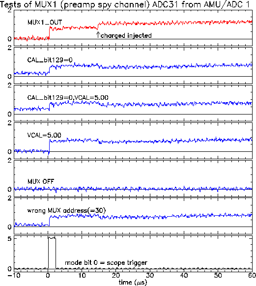
The plot (postscript version
here) below shows a series
of tests of the MUX control bits. In each case, the scope trigger
was mode bit 0, which initiated the bench cal procedure to inject charge
into a single preamp channel. These tests were all done on the first
TGV and AMU/ADC chips on the board. I tested this at the AMU/ADC output.
Red traces indicate that there should be a preamp signal.
Blue traces indicate that there should not be a preamp signal.
The first (top) plot shows MUX1_OUT with everything set up so that
there should be a signal seen. The first edge (at about 0 microsec)
is caused by the preamp reset. The second edge (marked with an arrow)
shows the charge injected. This example has VCAL=3.48 (meaning the
max charge injection possible), CAL_EN=1 (in the heap manager serial string),
CAL_EN_32=1 (bit 129 in TGV serial string), all other
CAL_EN_1--CAL_EN_31= 0,
MUX1_OE=MUX1_HIZ=1, and MUX1_0-4=11111.
The second plot shows MUX1_OUT with CAL_EN_32=0
(bit 129 in TGV serial string) -- meaning that there should be no
charge injected into
the preamp. All other bits were set as in the first plot.
As expected, no signal is seen.
The third plot shows MUX1_OUT with CAL_EN_32=0 and VCAL=5.00.
All other bits are set as in the first plot.
This means that the charge should not be injected into this
channel and furthermore, the charge to be injected is zero
(VCAL=5.00 corresponds to the minimum charge injection).
As expected, no signal is seen.
The fourth plot MUX1_OUT with VCAL=5.00.
All other bits are set as in the first plot.
This means that charge injection is enabled in this
channel, but the actual charge injection should be
(approximately) zero. As expected, no signal is
seen.
The fifth plot shows MUX1_OUT with MUX1_OE=MUX1_HIZ=0.
This means the MUX1 output is off. All other bits
are set as in the first plot. As expected, nothing,
not even the first edge (at 0 microsec) from the
preamp reset.
The sixth plot shows MUX1_OUT with MUX1_0-4=01111.
All other bits are set as in the first plot.
This means that the MUX looks at channel 30 of the TGV,
while the charge is being injected into channel 31.
As expected, no signal is seen.
The 7th (bottom) plot shows mode bit 0, which was
used to trigger the scope for all the other traces.
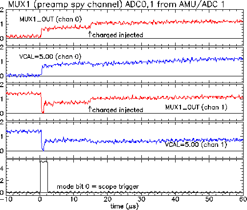
The plot (postscript version
here) below shows a few
tests to check how the address bit correspond to input
channel number.
The first (top) plot shows MUX1_OUT with
VCAL=3.48 (meaning the
max charge injection possible),
CAL_EN=1 (in the heap manager serial string),
CAL_EN_1=1 (bit 160 in TGV serial string), all other
CAL_EN_2--CAL_EN_32= 0,
MUX1_OE=MUX1_HIZ=1, and MUX1_0-4=00000.
In other words, a large amount of charge is being
injected into preamp channel 0 and the mux is setup
to look at channel 0. The arrow shows where the
edge from the charge injection appears.
The second plot shows MUX1_OUT with everything setup
as in the first plot except VCAL=5.00. This means that
(approximately) zero charge is injected with the bench
cal. As expected, no signal is seen.
The third plot is like the first plot, except now
the charge is injected into channel 1. This means
that CAL_EN_2=1 (preamp serial string) and MUX1_0-4=10000.
Again, the edge from the charge injection is seen at
the arrow.
The fourth plot is like the seond plot, except it shows
channel 1 with (approximately) no charge injected.
Again, no signal is seen.
The fifth (bottom) plot shows mode bit 0, which was
used to trigger the scope for all the other traces.
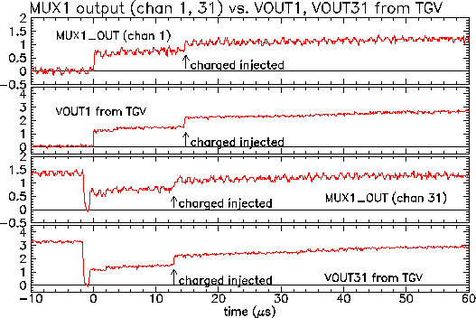
The plot (postscript version
here) below shows a
set of tests to verify that the MUX1 output looks like
the actual TGV output. Unlike the plots above, the following
plots do not use mode bit 0 as the scope trigger. They
are triggered by the preamp output signal, so time=0
does not have the same meaning as in the plots above.
The first two plots shows MUX1_OUT (top) and VOUT1 (2nd)
with VCAL=3.48 (meaning the
max charge injection possible),
CAL_EN=1 (in the heap manager serial string),
CAL_EN_2=1 (bit 159 in TGV serial string), all other
CAL_EN_2--CAL_EN_32= 0,
MUX1_OE=MUX1_HIZ=1, and MUX1_0-4=10000.
In other words, a large amount of charge is being
injected into preamp channel 1 and the mux is setup
to look at channel 1. VOUT1 is the output of the
preamp (into the AMU/ADC) from channel 1.
The arrow shows where the
edge from the charge injection appears on each plot.
Notice that the vertical scales are different.
It appears that the MUX does correspond to the
real TGV output, but the amplitude is lower (by a little
more than a factor of 2) and there is more noise
in the MUX1 output.
The third and fourth plots below are similar to
the first two, but show the same thing for
channel 31. Again, the MUX output is similar to the
TGV output, but with a lower amplitude and more noise.
John Sullivan
updated 5-Mar-1999