|

|
|
|
|

The plot (postscript version here) below shows some of the output signals from AMU/ADC 1. These were all measured using the "bench calibration", which is enabled with mode bit 2 and triggered by mode bit 0. The ADC_A0 (address bit zero) lines was used to trigger the scope for each trace shown.
10 bit digitization was used (SLCT0=0, SLCT1=1) with a 40 mHz 4x clock. The correlator was on (RAW_MODE=0).
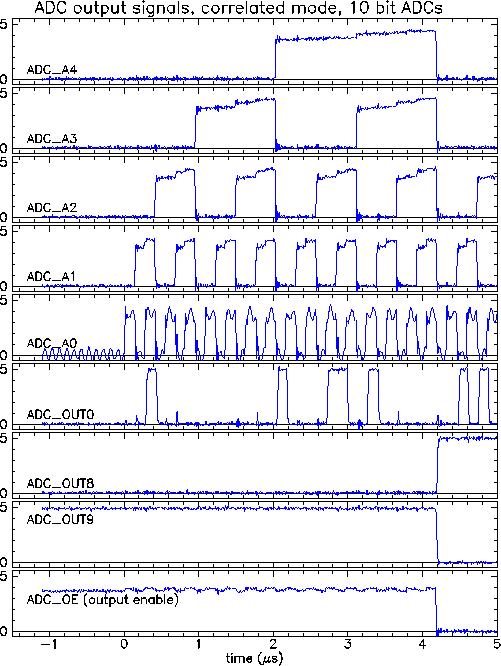
The top 5 traces show the address lines counting from ADC channel 0 to 31. The bottom lines shows ADC_OE -- the output enable for this ADC. After this line goes low, the address and data lines are controlled by another ADC chip.
It is possible to (partially) compare the data values seen
in the scope traces with results actually read out by the computer.
The data values were:
| channel number | value (hex) | channel number | value (hex) | channel number | value (hex) | channel number | value (hex) 0
| 216
| 8
| 218
| 16
| 219
| 24
| 218
| 1
| 218
| 9
| 218
| 17
| 218
| 25
| 217
| 2
| 216
| 10
| 21A
| 18
| 21A
| 26
| 21A
| 3
| 217
| 11
| 216
| 19
| 21A
| 27
| 216
| 4
| 216
| 12
| 21A
| 20
| 218
| 28
| 218
| 5
| 218
| 13
| 216
| 21
| 217
| 29
| 218
| 6
| 216
| 14
| 218
| 22
| 21B
| 30
| 218
| 7
| 218
| 15
| 218
| 23
| 216
| 31
| 218
| |
From these scope trace, it is possible to see that (counting from 0), word numbers 3, 16, 21, 22, 25 have bit 0 set -- meaning they should be odd numbers. The others should be even. Looking at the table of data, this is exactly what is seen. Also, bit 9 should always be set and bit 8 should never be set in the output data -- again this is exactly what is seen (bit 9=1 and bit 8=0 gives the intial "2" in exact ADC value).
The plots above also show that the address lines are counting correctly.
Although it is not shown here, I looked to see that ADC_OE appears at the end of the output sequence for the last TGV chip. I did not check the ones in between, but it appears that this is counting correctly.