|

|
|
|
|
DCIM/TCIM clock signals
We are having problems keeping the Glinks locked on the MVD DCIM boards. The problem has been that the Glinks will not stay locked consistently. The following plots were made to try to understand where the problem comes from.
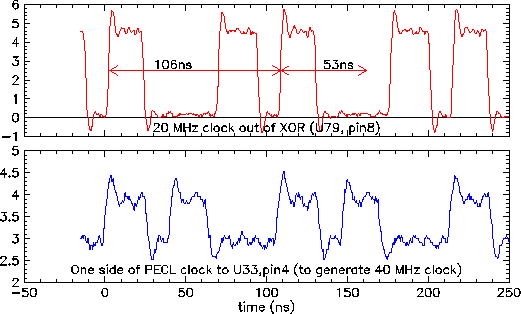
The following pair of plots shows what I think might be the problem. The "20 MHz" (actually about 18.8 MHz) clock does not look very good. The top plot shows the 20 MHz clock at the output of U79, pin 8 (an XOR, 74ACT88) on the DCIM board. All of the other 20 MHz and 40 MHz clocks on the board seem to descend from this clock. The input to this is a "10 MHz" clock, which is delayed and then "XOR'ed" in this chip. The 20 MHz clock is used by the Glink transmiter chips (hdmp-1022). The bottom plot in this pair is a PECL version of the same clock. I believe that this PECL clock is used to generated the 40 MHz clock for the Xilinx FPGAs.
The unequally spaced signals on the "20 MHz" clock are apparantly caused by the unequal duty factor in the two signals (delayed 10 MHz and undelayed 10 MHz) which are used to generate the 20 MHz clock. This pair of signals (triggered on the top plot) is shown below. Notice that the signals is "high" longer than it is "low". This seems to be the origin of the unequally spaced clock pulses above.

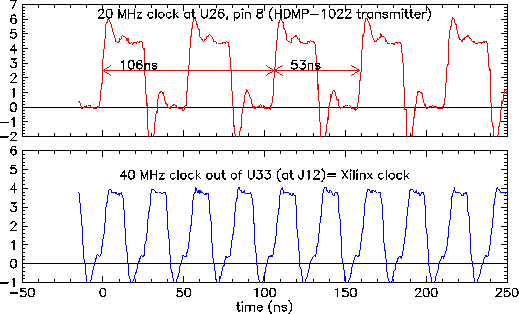
While I think this funny-looking clock is a problem, the following pair of plots does not really support my belief. The top plot above shows the 20 MHz clock at U26, pin 8 -- the HPMP-1022 Glink transmitter chip. This clock, which is derived from the ugly clock above, looks better. The bottom plot shows the 40 MHz clock at test point J-12. This is the 40 MHz clock out of U33 (SY89429JC) which goes to the Xilinx chips. It is derived from the ugly PECL clock above. Either I am wrong about this being a problem, or these clocks occaisonally lose a tick but usually look good.
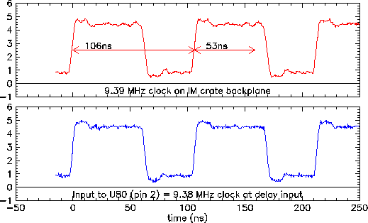
Next, I looked at the 10 MHz clock on the backplane of the interface module crate. The strange duty factor on the clock seemed to be there. This is the signal which is input the the DCIM board. This signal is the top plot in the pair below. The bottom plot below is the 10 MHz clock at the input to the delay circuit for one side of the 10 MHz clock. Specifically, it is shown at U80, pin 2.
I continued to assume that the stange duty factor in the clock was a problem. The clock on the backplane comes from the TCIM. So, I looked at the clock on the TCIM. The top plot below shows the 10 MHz clock at the output of U12 (pin 15). This is a 74ACT827. The signal goes from this pin, via a 22 ohm resisitor, to pin 10 on the backplane -- in other words the signal on the backplane shown above. The bottom plot in the pair below is the input signal at U12 (pin 10).

I did not really trace the signal the whole way through the TCIM. Roughly, the path seems to be Glink input -- U28, pin 6 (input to a PDU14F-4) -- U28, pin 1 (output) -- U29 pin 6 (another input to a PDU14F-4) -- U29 pin 1 (output, actually OUT-BAR) -- U30, inputs 5-8 (U30 is a 74ACT541) -- U30, outputs 12-15 (DELAY_CLK0 -- DELAY_CLK3) -- following DELAY_CLK2, it goes to many places, including U22 pin 3 (a 74ACT74). I looked at the clock at U22 pin 3 and at U29 pin 1. Those are shown below.
